LM3310SQ/NOPB National Semiconductor, LM3310SQ/NOPB Datasheet
LM3310SQ/NOPB
Specifications of LM3310SQ/NOPB
LM3310SQNOPB
LM3310SQNOPBTR
LM3310SQNOPBTR
LM3310SQTR


Related parts for LM3310SQ/NOPB

LM3310SQ/NOPB Summary of contents
Page 1
... The gate pulse modulation switch can operate with a VGH voltage 30V. The LM3310 is available in a low profile 24-lead LLP package. Typical Application Circuit © 2007 National Semiconductor Corporation Features ■ Boost converter with a 2A, 0.18Ω switch ■ ...
Page 2
Connection Diagram Ordering Information Order Number Spec. LM3310SQ LM3310SQX LM3310SQ NOPB LM3310SQX NOPB Pin Descriptions Pin Name 1 NC Not internally connected. Leave pin open. 2 VGHM Output of GPM circuit. This output directly drives the supply for the gate ...
Page 3
Pin Name 14 SS Boost converter soft start pin Boost compensation network connection. Connected to the output of the voltage error amplifier FREQ Switching frequency select input. Connect this pin to V 660kHz operation ...
Page 4
www.national.com 20133359 4 20133358 ...
Page 5
... Absolute Maximum Ratings If Military/Aerospace specified devices are required, please contact the National Semiconductor Sales Office/ Distributors for availability and specifications Voltage FB Voltage V Voltage (Note 2) C SHDN Voltage FREQ AV IN Amplifier Inputs/Output VGH Voltage VGHM Voltage VFLK, VDPM, V Voltage DD CE Voltage (Note 2) ...
Page 6
Electrical Characteristics Specifications in standard type face are for T Range ( T = −40°C to +125°C). Unless otherwise specified V J Operational Amplifier Symbol Parameter V Input Offset Voltage OS I Input Bias Current (POS Pin Swing ...
Page 7
Note 9: Bias current flows into pin. Typical Performance Characteristics SHDN Pin Current vs. SHDN Pin Voltage FREQ Pin Current vs. Input Voltage CE Pin Current vs. Input Voltage SS Pin Current vs. Input Voltage 20133361 FB Pin Current vs. ...
Page 8
VFLK Pin Current vs. VFLK Pin Voltage 1.28MHz Switching Quiescent Current vs. Input Voltage 1.28MHz Switching Quiescent Current vs. Temperature www.national.com 660kHz Switching Quiescent Current vs. Input Voltage 20133366 660kHz Switching Quiescent Current vs. Temperature 20133367 660kHz Switching Frequency vs. ...
Page 9
Switching Frequency vs. Temperature Non-Switching Quiescent Current vs. Input Voltage GPM Disabled Non-Switching Quiescent Current vs. Temperature GPM Disabled Switch Current Limit vs. Input Voltage 20133369 Non-Switching Quiescent Current vs. Input Voltage GPM Enabled 20133371 Non-Switching Quiescent Current vs. ...
Page 10
Power NMOS R vs. Input Voltage DSON 1.28MHz Max. Duty Cycle vs. Input Voltage 1.28MHz Max. Duty Cycle vs. Temperature www.national.com 660kHz Max. Duty Cycle vs. Input Voltage 20133375 660kHz Max. Duty Cycle vs. Temperature 20133383 1.28MHz Application Efficiency 20133376 ...
Page 11
Application Efficiency VGH Pin Bias Current vs. VGH Pin Voltage VGHM-RE PMOS R vs. VGHM Pin Voltage DSON VGH Pin Bias Current vs. VGH Pin Voltage 20133326 VGH-VGHM PMOS R 20133378 VGHM OFF Resistance vs. Temperature 20133380 11 20133377 ...
Page 12
Op-Amp Source Current vs. AV Op-Amp Quiescent Current vs. AV Op-Amp Offset Voltage vs. Load Current www.national.com Op-Amp Sink Current vs 20133396 Op-Amp Offset Voltage vs 20133316 1.28MHz, 8.5V Application Boost Load Step V = 8.5V, ...
Page 13
Application Boost Startup Waveform = 20Ω 8.5V 3.3V 20µF, R OUT IN OUT LOAD 2V/div, DC SHDN 5V/div, DC OUT 500mA/div, DC ...
Page 14
Operation (a) First Cycle of Operation (b) Second Cycle Of Operation CONTINUOUS CONDUCTION MODE The LM3310 contains a current-mode, PWM boost regulator. A boost regulator steps the input voltage higher output voltage. In continuous conduction mode (when ...
Page 15
UVP circuitry will prevent the device from switching if the input voltage present is lower than the UVP On threshold. During normal operation the UVP circuitry will disable the device if the input voltage falls ...
Page 16
V is some voltage connected to the resistor divider on X pin typically connected to the output of the boost DD X switching regulator. When PMOS switch P3 turns off, VGHM will be high impedance ...
Page 17
R is the output impedance of the error amplifier, ap- O proximately 900kΩ. For most applications, performance can be optimized by choosing values within the range 5kΩ ≤ 100kΩ (R can 200kΩ Output ...
Page 18
INPUT AND OUTPUT CAPACITOR SELECTION The switching action of a boost regulator causes a triangular voltage waveform at the input. A capacitor is required to re- duce the input ripple and noise for proper operation of the regulator. The size ...
Page 19
POWER DISSIPATION The output power of the LM3310 is limited by its maximum power dissipation. The maximum power dissipation is deter- mined by the formula )/θ jmax A JA where T is the maximum ...
Page 20
FIGURE 7. Evaluation Board Layout (top layer) 20 20133324 ...
Page 21
FIGURE 8. Evaluation Board Layout (bottom layer) 21 20133325 www.national.com ...
Page 22
FIGURE 9. Li-Ion to 8V, 1.28MHz Application 22 20133329 ...
Page 23
FIGURE 10 10.5V, 1.28MHz Application Some Recommended Inductors (Others May Be Used) Manufacturer Coilcraft TDK Pulse Sumida CDRH8D28 and CDRH8D43 series Some Recommended Input And Output Capacitors (Others May Be Used) Manufacturer Vishay Sprague 293D, 592D, and 595D ...
Page 24
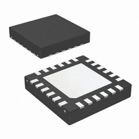
Physical Dimensions www.national.com inches (millimeters) unless otherwise noted LLP-24 Pin Package (SQA) For Ordering, Refer to Ordering Information Table NS Package Number SQA24A 24 ...
Page 25
Notes 25 www.national.com ...
Page 26
... For more National Semiconductor product information and proven design tools, visit the following Web sites at: Products Amplifiers www.national.com/amplifiers Audio www.national.com/audio Clock Conditioners www.national.com/timing Data Converters www.national.com/adc Displays www.national.com/displays Ethernet www.national.com/ethernet Interface www.national.com/interface LVDS www.national.com/lvds Power Management www.national.com/power Switching Regulators www.national.com/switchers LDOs www ...