LM3524DN/NOPB National Semiconductor, LM3524DN/NOPB Datasheet - Page 9
LM3524DN/NOPB
Manufacturer Part Number
LM3524DN/NOPB
Description
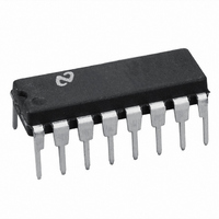
IC REGULATOR PWM SWITCHER 16-DIP
Manufacturer
National Semiconductor
Type
Step-Down (Buck), Step-Up (Boost), Flybackr
Datasheet
1.LM2524DNNOPB.pdf
(22 pages)
Specifications of LM3524DN/NOPB
Internal Switch(s)
Yes
Synchronous Rectifier
No
Number Of Outputs
1
Voltage - Output
5V
Current - Output
200mA
Frequency - Switching
550kHz
Voltage - Input
8 ~ 40 V
Operating Temperature
0°C ~ 125°C
Mounting Type
Through Hole
Package / Case
16-DIP (0.300", 7.62mm)
Power - Output
1W
Lead Free Status / RoHS Status
Lead free / RoHS Compliant
Other names
*LM3524DN
LM3524DN
LM3524DN


The output of the amplifier, or input to the pulse width modu-
lator, can be overridden easily as its output impedance is very
high (Z
to pin 9 which will override the error amplifier and force a par-
ticular duty cycle to the outputs. An example of this could be
a non-regulating motor speed control where a variable volt-
age was applied to pin 9 to control motor speed. A graph of
the output duty cycle vs the voltage on pin 9 is shown in Figure
5.
The duty cycle is calculated as the percentage ratio of each
output's ON-time to the oscillator period. Paralleling the out-
puts doubles the observed duty cycle.
The amplifier's inputs have a common-mode input range of
1.5V–5.5V. The on board regulator is useful for biasing the
inputs to within this range.
O
5 MΩ). For this reason a DC voltage can be applied
FIGURE 5.
865008
9
CURRENT LIMITING
The function of the current limit amplifier is to override the
error amplifier's output and take control of the pulse width.
The output duty cycle drops to about 25% when a current limit
sense voltage of 200 mV is applied between the +C
−C
mately 5% results in a 0% output duty cycle. Care should be
taken to ensure the −0.7V to +1.0V input common-mode
range is not exceeded.
In most applications, the current limit sense voltage is pro-
duced by a current through a sense resistor. The accuracy of
this measurement is limited by the accuracy of the sense re-
sistor, and by a small offset current, typically 100 μA, flowing
from +CL to −CL.
OUTPUT STAGES
The outputs of the LM3524D are NPN transistors, capable of
a maximum current of 200 mA. These transistors are driven
180° out of phase and have non-committed open collectors
and emitters as shown in Figure 6.
L
sense terminals. Increasing the sense voltage approxi-
FIGURE 6.
865009
www.national.com
L
and
Related parts for LM3524DN/NOPB
Image
Part Number
Description
Manufacturer
Datasheet
Request
R

Part Number:
Description:
ENHANCED PWM CONTROLLER, 3524, DIP
Manufacturer:
National Semiconductor
Datasheet:
Part Number:
Description:
National Semiconductor [8-Bit D/A Converter]
Manufacturer:
National Semiconductor
Datasheet:
Part Number:
Description:
National Semiconductor [Media Coprocessor]
Manufacturer:
National Semiconductor
Datasheet:
Part Number:
Description:
Digitally Controlled Tone and Volume Circuit with Stereo Audio Power Amplifier, Microphone Preamp Stage and National 3D Sound
Manufacturer:
National Semiconductor
Datasheet:
Part Number:
Description:
Digitally Controlled Tone and Volume Circuit with Stereo Audio Power Amplifier, Microphone Preamp Stage and National 3D Sound
Manufacturer:
National Semiconductor
Datasheet:
Part Number:
Description:
AC97 Rev 2 Codec with Sample Rate Conversion and National 3D Sound
Manufacturer:
National Semiconductor
Part Number:
Description:
Manufacturer:
National Semiconductor
Datasheet:
Part Number:
Description:
Manufacturer:
National Semiconductor
Datasheet:
Part Number:
Description:
General Purpose, Low Voltage, Low Power, Rail-to-Rail Output Operational Amplifiers
Manufacturer:
National Semiconductor
Datasheet:
Part Number:
Description:
8-bit 20 MSPS flash A/D converter.
Manufacturer:
National Semiconductor
Datasheet:
Part Number:
Description:
Low Noise Quad Operational Amplifier
Manufacturer:
National Semiconductor
Datasheet:
Part Number:
Description:
Quad Differential Line Receivers
Manufacturer:
National Semiconductor
Datasheet:
Part Number:
Description:
Quad High Speed Trapezoidal? Bus Transceiver
Manufacturer:
National Semiconductor
Datasheet:
Part Number:
Description:
Dual Line Receiver
Manufacturer:
National Semiconductor
Datasheet: