LM4510SDX/NOPB National Semiconductor, LM4510SDX/NOPB Datasheet
LM4510SDX/NOPB
Specifications of LM4510SDX/NOPB
Available stocks


Related parts for LM4510SDX/NOPB


LM4510SDX/NOPB Summary of contents
Page 1
... The LM4510 is available in a 10-pin thermally enhanced Leadless Leadframe Package: LLP-10. Typical Application Circuit © 2010 National Semiconductor Corporation LM4510 Features ■ 18V@80 mA from 3.2V input ■ ...
Page 2
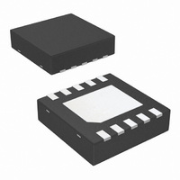
Connection Diagram Ordering Information Order Number SPEC Package Type LM4510SD NOPB LLP-10 LM4510SDX NOPB LLP-10 www.national.com Efficiency 16V OUT LLP-10 No Pullback Package, 3mm x 3mm x 0.8mm NS Package Number SDA10A NSC Package Drawing SDA10A SDA10A ...
Page 3
Pin Descriptions/Functions Pin Name 1 SW Switch pin. Drain connections of both internal NMOS and PMOS devices. 2 PGND Power ground 3 VIN Analog and Power supply input. Input range: 2.7V to 5.5V Enable logic input. HIGH= Enabled, ...
Page 4
... Absolute Maximum Ratings 2) If Military/Aerospace specified devices are required, please contact the National Semiconductor Sales Office/ Distributors for availability and specifications. VIN VOUT SW (Note 3) EN, SS, COMP FB PGND to AGND Continuous Power Dissipation (Note 4) Junction Temperature (T ) J-MAX Storage Temperature Range ( Lead Temperature (Soldering, 10 sec) ...
Page 5
... J Note 5: For detailed soldering information and specifications, please refer to National Semiconductor Application Note 1187: Leadless Leadframe Package (LLP) , available at www.national.com. Note 6: In applications where high power dissipation and/or poor package thermal resistance is present, the maximum ambient temperature may have to be derated ...
Page 6
Typical Performance Characteristics LM4510SD, Circuit of Figure 1, (L=4.7 µH, COILCRAFT, DO3316-472ML; C 12103D106KAT2A; C =10 nF, TDK, C1608C0G1E103J 9t06031A4642FBHFT), V =3.6V Switching Quiescent Current vs V Load Capabilty ...
Page 7
Switching Frequency vs Temperature Load Regulation ( OUT Line Regulation ( OUT Load Regulation (V 30031011 Line Regulation (V 30031034 Efficiency vs Output Current (V 30031033 OUT ...
Page 8
Efficiency vs Output Current ( OUT Line Transient Response ( OUT Start OUT LOAD www.national.com 30031031 30031003 = 530 Ω) 30031007 8 Efficiency vs Output Current ...
Page 9
Short Circuit Response ( OUT 30031008 Output Voltage Ripple ( 100 mA) OUT OUT 30031099 Output Voltage Ripple ( mA) OUT OUT 9 30031098 www.national.com ...
Page 10
Block Diagram Operation Description LM4510 is a peak current-mode, fixed-frequency PWM boost regulator that employs both Non-Synchronous Switching. The DC/DC regulator regulates the feedback output voltage providing excellent line and load transient response. The op- eration of the LM4510 can ...
Page 11
Synchronous boost converter is shown in Figure 3. At the start of each cycle, the oscillator sets the driver logic and turns on the NMOS power device and turns off the PMOS power de- vice. Cycle 1 Description Refer to ...
Page 12
MAXIMUM OUTPUT CURRENT When the output voltage is set at different level important to know the maximum load capability. By first order estima- tion, I can be estimated by the following equation: OUT(MAX) INDUCTOR SELECTION The larger value ...
Page 13
TABLE 3. Suggested C Model 4.7 µF for C IN C2012X5R0J475 GRM21BR60J475 JMK212BJ475 C2012X5R0J475K 10 µF for C OUT TMK316BJ106KL 12103D106KAT2A SOFT-START FUNCTION AND SOFT-START CAPACITOR SELECTION The LM4510 has a soft-start pin that can be used to limit the ...
Page 14
LAYOUT CONSIDERATIONS AND THERMAL MANAGEMENT FIGURE 7. Evaluation Board Layout High frequency switching regulators require very careful lay- out of components in order to get stable operation and low noise. All components must be as close as possible to the ...
Page 15
Physical Dimensions inches (millimeters) unless otherwise noted For Ordering, Refer to Ordering Information Table 10-pin LLP Package NS Package Number SDA10A 3mm x 3mm x 0.8mm 15 www.national.com ...
Page 16
... For more National Semiconductor product information and proven design tools, visit the following Web sites at: www.national.com Products Amplifiers www.national.com/amplifiers Audio www.national.com/audio Clock and Timing www.national.com/timing Data Converters www.national.com/adc Interface www.national.com/interface LVDS www.national.com/lvds Power Management www.national.com/power Switching Regulators www.national.com/switchers LDOs www.national.com/ldo LED Lighting www ...