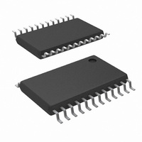
LM2716MTX/NOPB National Semiconductor, LM2716MTX/NOPB Datasheet

LM2716MTX/NOPB
Specifications of LM2716MTX/NOPB
Related parts for LM2716MTX/NOPB
LM2716MTX/NOPB Summary of contents
Page 1
... Each converter may also be shut down indepen- dently with its own shutdown pin. The LM2716 is available in a low profile 24-lead TSSOP package. Typical Application Circuit © 2005 National Semiconductor Corporation Features n Fixed 3.3V buck converter with a 1.8A, 0.16Ω, internal switch n Adjustable boost converter with a 3.6A, 0.12Ω ...
Page 2
Connection Diagram Ordering Information Order Number LM2716MT LM2716MTX www.national.com Top View 20071204 24-Lead TSSOP Package Type NSC Package Drawing TSSOP-24 MTC24 TSSOP-24 MTC24 2 Supplied As 61 Units, Rail 2500 Units, Tape and Reel ...
Page 3
Pin Descriptions Pin Name 1 PGND Power ground. AGND and PGND pins must be connected together directly at the part. 2 FB1 Buck output voltage feedback input Buck compensation network connection. Connected to the output of the voltage ...
Page 4
Block Diagram www.national.com 4 20071203 ...
Page 5
... Absolute Maximum Ratings If Military/Aerospace specified devices are required, please contact the National Semiconductor Sales Office/ Distributors for availability and specifications SW1 Voltage SW2 Voltage FB1 Voltage FB2 Voltage V Voltage C1 0.965V ≤ Voltage C2 SHDN1 Voltage SHDN2 Voltage SS1 Voltage SS2 Voltage FSLCT Voltage ...
Page 6
Electrical Characteristics Specifications in standard type face are for T ture Range (T = −40˚C to +125˚C) Unless otherwise specified Symbol Parameter Th Buck SHDN Threshold SHDN1 Th Boost SHDN Threshold SHDN2 I Buck Soft Start Pin Current ...
Page 7
Typical Performance Characteristics Switching Frequency vs. R Switching Frequency vs. Input Voltage (F = 600kHz) SW Buck Efficiency vs. Load Current (F = 600kHz) SW Switching Frequency vs. Input Voltage Resistor F 20071223 Buck Efficiency vs. Load Current 20071225 Boost ...
Page 8
Typical Performance Characteristics Boost Efficiency vs. Load Current (F = 600kHz) SW www.national.com (Continued) Boost Switch R 20071232 8 vs. Input Voltage DSON 20071235 ...
Page 9
Buck Operation PROTECTION (BOTH REGULATORS) The LM2716 has dedicated protection circuitry running dur- ing normal operation to protect the IC. The Thermal Shut- down circuitry turns off the power devices when the die temperature reaches excessive levels. The UVP comparator ...
Page 10
Buck Operation (Continued) COMPENSATION COMPONENTS In the control to output transfer function, the first pole F can be estimated as 1/(2πR C OUT OUT the output capacitor is 1/(2πESRC OUT frequency pole F in the range of 45kHz to 150kHz: ...
Page 11
Boost Operation FIGURE 1. Simplified Boost Converter Diagram (a) First Cycle of Operation (b) Second Cycle Of Operation CONTINUOUS CONDUCTION MODE The LM2716 contains a current-mode, PWM boost regulator. A boost regulator steps the input voltage higher ...
Page 12
Boost Operation (Continued) The LM2716 has a current mode PWM boost converter. The signal flow of this control scheme has two feedback loops, one that senses switch current and one that senses output voltage. To keep a current programmed control ...
Page 13
Boost Operation (Continued) Resistance, denoted R ) capacitors be used such as ESR ceramic, polymer electrolytic, or low ESR tantalum. Higher ESR capacitors may be used but will require more compen- sation which will be explained later on in the ...
Page 14
Boost Operation (Continued 0.072F (in V/s) SW where R is the minimum load resistance mum input voltage the error amplifier transconduc- m tance found in the Electrical Characteristics table, and R is the value ...
Page 15
Application Information (Continued) FIGURE 3. 15V, 3.3V Output Application 15 20071257 www.national.com ...
Page 16
Application Information www.national.com (Continued) FIGURE 4. PCB Layout, Top 16 20071258 ...
Page 17
Application Information (Continued) FIGURE 5. PCB Layout, Bottom 17 20071259 www.national.com ...
Page 18
... BANNED SUBSTANCE COMPLIANCE National Semiconductor manufactures products and uses packing materials that meet the provisions of the Customer Products Stewardship Specification (CSP-9-111C2) and the Banned Substances and Materials of Interest Specification (CSP-9-111S2) and contain no ‘‘Banned Substances’’ as defined in CSP-9-111S2. ...


