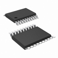
LM26003MHX/NOPB National Semiconductor, LM26003MHX/NOPB Datasheet - Page 17

LM26003MHX/NOPB
Manufacturer Part Number
LM26003MHX/NOPB
Description
IC REG BUCK SW 3A 20-TSSOP
Manufacturer
National Semiconductor
Series
PowerWise®r
Type
Step-Down (Buck)r
Datasheet
1.LM26003QMHNOPB.pdf
(20 pages)
Specifications of LM26003MHX/NOPB
Internal Switch(s)
Yes
Synchronous Rectifier
No
Number Of Outputs
1
Voltage - Output
1.25 ~ 35 V
Current - Output
3A
Frequency - Switching
150kHz ~ 500kHz
Voltage - Input
4 ~ 38 V
Operating Temperature
-40°C ~ 125°C
Mounting Type
Surface Mount
Package / Case
20-TSSOP Exposed Pad, 20-eTSSOP, 20-HTSSOP
Power - Output
3.1W
Lead Free Status / RoHS Status
Lead free / RoHS Compliant
Other names
LM26003MHX
Available stocks
Company
Part Number
Manufacturer
Quantity
Price
Company:
Part Number:
LM26003MHX/NOPB
Manufacturer:
ST
Quantity:
445
Part Number:
LM26003MHX/NOPB
Manufacturer:
TI/德州仪器
Quantity:
20 000
GND pin must be connected to ground. This quieter plane
should be connected to the high current ground plane at a
quiet location, preferably near the Vout ground as shown by
the dashed line in
The EP GND plane should be made as large as possible,
since it is also used for thermal dissipation. Several vias can
be placed directly below the EP to increase heat flow to other
layers when they are available. The recommended via hole
diameter is 0.3mm.
The trace from the FB pin to the resistor divider should be
short and the entire feedback trace must be kept away from
the inductor and switch node. See Application Note AN-1229
for more information regarding PCB layout for switching reg-
ulators.
Thermal Considerations and TSD
Although the LM26003 has a built in current limit, at ambient
temperatures above 80°C, device temperature rise may limit
the actual maximum load current. Therefore, temperature rise
must be taken into consideration to determine the maximum
allowable load current.
Temperature rise is a function of the power dissipation within
the device. The following equations can be used to calculate
power dissipation (PD) and temperature rise, where total PD
is the sum of FET switching losses, FET DC losses, drive
losses, Iq, and VBIAS losses:
PD
TOTAL
= Psw
Figure
AC
+ Psw
11.
DC
+ PQG + P
Iq
+ P
VBIAS
17
Given this total power dissipation, junction temperature can
be calculated as follows:
Where θ
with a large copper plane area. θ
metallization area.
To calculate the maximum allowable power dissipation, as-
sume Tj = 125°C. To ensure that junction temperature does
not exceed the maximum operating rating of 125°C, power
dissipation should be verified at the maximum expected op-
erating frequency, maximum ambient temperature, and min-
imum and maximum input voltage. The calculated maximum
load current is based on continuous operation and may be
exceeded during transient conditions.
If the power dissipation remains above the maximum allow-
able level, device temperature will continue to rise. When the
junction temperature exceeds its maximum, the LM26003 en-
gages Thermal Shut Down (TSD). In TSD, the part remains
in a shutdown state until the junction temperature falls to with-
in normal operating limits. At this point, the device restarts in
soft-start mode.
Psw
JA
DC
= 32°C/W (typically) when using a multi-layer board
= D x Iload
P
Tj = Ta + (PD
QG
P
VBIAS
= Vin x 9.2 x 10
2
P
x (0.095 + 0.00065 x (T
Iq
= Vbias x I
= Vin x Iq
TOTAL
JA
varies with board type and
VBIAS
-9
x θ
x fsw
JA
)
www.national.com
j
- 25))


