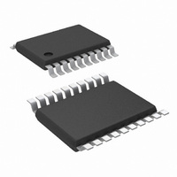
LM5118Q1MHX/NOPB National Semiconductor, LM5118Q1MHX/NOPB Datasheet - Page 21

LM5118Q1MHX/NOPB
Manufacturer Part Number
LM5118Q1MHX/NOPB
Description
IC BUCK BST ADJ 20TSSOP
Manufacturer
National Semiconductor
Series
PowerWise®r
Type
Step-Down (Buck), Step-Up (Boost)r
Datasheet
1.LM5118MHXNOPB.pdf
(26 pages)
Specifications of LM5118Q1MHX/NOPB
Internal Switch(s)
No
Synchronous Rectifier
Yes
Number Of Outputs
1
Voltage - Output
1.23 ~ 70 V
Frequency - Switching
200kHz, 515kHz
Voltage - Input
3 ~ 75 V
Operating Temperature
-40°C ~ 125°C
Mounting Type
Surface Mount
Package / Case
20-TSSOP Exposed Pad, 20-eTSSOP, 20-HTSSOP
Lead Free Status / RoHS Status
Lead free / RoHS Compliant
Current - Output
-
Power - Output
-
Other names
LM5118Q1MHX
Available stocks
Company
Part Number
Manufacturer
Quantity
Price
Company:
Part Number:
LM5118Q1MHX/NOPB
Manufacturer:
BROADCOM
Quantity:
101
Company:
Part Number:
LM5118Q1MHX/NOPB
Manufacturer:
NS/TI
Quantity:
2 600
The plots shown in Figures 13, 14 and 15 illustrate the gain
and phase diagrams of the design example. The overall band-
width is lower in a buck-boost application due the compen-
sation challenges associated with the right-half-plane zero.
For a pure buck application, the bandwidth could be much
higher. The LM5116 datasheet is a good reference for com-
pensation design of a pure buck mode regulator.
Bias Power Dissipation Reduction
Buck or Buck-boost regulators operating with high input volt-
age can dissipate an appreciable amount of power while
supplying the required bias current of the IC. The VCC regu-
lator must step-down the input voltage VIN to a nominal VCC
level of 7V. The large voltage drop across the VCC regulator
FIGURE 16. VCC Bias from VOUT 4V < VOUT < 15V
FIGURE 15. Overall Loop Gain and Phase
21
translates into high power dissipation in the VCC regulator.
There are several techniques that can significantly reduce this
bias regulator power dissipation. Figures 16 and 17 depict two
methods to bias the IC, one from the output voltage and one
from a separate bias supply. In the first case, the internal VCC
regulator is used to initially bias the VCC pin. After the output
voltage is established, the VCC pin bias current is supplied
through the VCCX pin, which effectively disables the internal
VCC regulator. Any voltage greater than 4.0V can supply
VCC bias through the VCCX pin. However, the voltage ap-
plied to the VCCX pin should never exceed 15V. The voltage
supplied through VCCX must be large enough to drive the
switching MOSFETs into full saturation.
30058550
30058551
www.national.com


