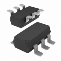
MAX1720EUTG ON Semiconductor, MAX1720EUTG Datasheet - Page 17

MAX1720EUTG
Manufacturer Part Number
MAX1720EUTG
Description
IC INVERTER CHRG PUMP VOLT 6TSOP
Manufacturer
ON Semiconductor
Type
Switched Capacitor (Charge Pump), Invertingr
Datasheet
1.MAX1720EUTG.pdf
(18 pages)
Specifications of MAX1720EUTG
Internal Switch(s)
Yes
Synchronous Rectifier
No
Number Of Outputs
1
Voltage - Output
-1.5 ~ -5.5 V, 3 ~ 11 V
Current - Output
50mA
Frequency - Switching
12kHz
Voltage - Input
1.5 ~ 5.5 V
Operating Temperature
-40°C ~ 85°C
Mounting Type
Surface Mount
Package / Case
SC-74-6
Power - Output
313mW
Function
Inverting
Output Voltage
- 5.5 V to - 1.15 V
Output Current
100 mA
Maximum Operating Temperature
+ 150 C
Mounting Style
SMD/SMT
Operating Supply Voltage (min)
1.15V
Operating Supply Voltage (max)
5.5V
Package Type
TSOP
Pin Count
6
Mounting
Surface Mount
Lead Free Status / RoHS Status
Lead free / RoHS Compliant
Other names
MAX1720EUTGOS
Available stocks
Company
Part Number
Manufacturer
Quantity
Price
Company:
Part Number:
MAX1720EUTG
Manufacturer:
ON Semiconductor
Quantity:
1 150
constructed by incorporating combinations of the former circuits. The converter shown above combines Figures 26 and 32 to
form a regulated negative output inverter with a non−regulated positive output doubler. The magnitude of −V
by the resistor values and follows the relationship −V
its output voltage will increase as the negative output load increases. This cross regulation characteristic is shown in the upper
portion of Figure 50. The dashed line is the open loop and the solid line is the closed loop configuration for the load regulation.
The load regulation for the positive doubler with a constant load on the −V
All of the previously shown converter circuits have only single outputs. Applications requiring multiple outputs can be
−3.0
−4.0
−5.0
9.0
8.0
0
I
Negative Inverter
out
, NEGATIVE INVERTER OUTPUT CURRENT (mA)
Tape & Reel Specifications Table
Figure 50. Load Regulation, Output
TSOP−6
Package
Voltage vs. Output Current
10
SHDN
PIN 1
Figure 52. Inverter Circuit Board Layout, Top View Copper Side
GND
V
Component Taping Orientation for TSOP−6 Devices
in
MARKING
R
R
R1 = 10 k, R2 = 20 k
T
DEVICE
A
out
out
Tape Width (W)
= 25°C
= 45 W − Open Loop
= 2 W − Closed Loop
8 mm
Positive Doubler
I
out
20
Standard Reel Component Orientation
= 15 mA
C
+
3
Inverter Size = 0.5 in x 0.2 in
Area = 0.10 in
(Mark Right Side Up)
http://onsemi.com
ref
TAPING FORM
IC1
USER DIRECTION OF FEED
(R
MAX1720
Pitch (P)
2
4 mm
30
/R
0.5″
17
1
2
, 64.5 mm
+ 1). Since the positive output is not within the feedback loop,
C
+
1
10.0
8.0
7.0
9.0
0
2
Part Per Full Reel
C
I
out
Negative Inverter I
R
R
T
+
2
A
1
2
out
, POSITIVE DOUBLER OUTPUT CURRENT (mA)
= 25°C
= 10 kW
= 20 kW
3000
is shown in Figure 51.
Figure 51. Load Regulation, Output
10
Voltage vs. Output Current
−V
GND
out
out
20
= 15 mA
Diameter
7 inches
30
out
40
is controlled
50


