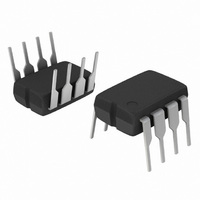
LM2574N-015G ON Semiconductor, LM2574N-015G Datasheet - Page 19

LM2574N-015G
Manufacturer Part Number
LM2574N-015G
Description
IC REG SW 0.5A 15V OUTPUT 8-DIP
Manufacturer
ON Semiconductor
Type
Step-Down (Buck)r
Datasheet
1.LM2574N-3.3G.pdf
(26 pages)
Specifications of LM2574N-015G
Internal Switch(s)
Yes
Synchronous Rectifier
No
Number Of Outputs
1
Voltage - Output
15V
Current - Output
500mA
Frequency - Switching
52kHz
Voltage - Input
4.75 ~ 40 V
Operating Temperature
-40°C ~ 125°C
Mounting Type
Through Hole
Package / Case
8-DIP (0.300", 7.62mm)
Output Voltage
15 V
Output Current
0.5 A
Input Voltage
4.75 V to 40 V
Switching Frequency
52 KHz
Operating Temperature Range
- 40 C to + 125 C
Mounting Style
Through Hole
Duty Cycle (max)
98 %
Lead Free Status / RoHS Status
Lead free / RoHS Compliant
Power - Output
-
Lead Free Status / Rohs Status
Lead free / RoHS Compliant
Available stocks
Company
Part Number
Manufacturer
Quantity
Price
Company:
Part Number:
LM2574N-015G
Manufacturer:
ON Semiconductor
Quantity:
135
supplied by the input capacitor C
Design Recommendations:
than the buck converter and so a different design procedure
has to be used to select the inductor L1 or the output
capacitor C
normally required for buck converter designs. Low input
voltages or high output currents require a large value output
capacitor (in the range of thousands of mF).
inverting converter design is between 68 mH and 220 mH. To
select an inductor with an appropriate current rating, the
inductor peak current has to be calculated.
current:
conditions, the worst case occurs when V
situations, the delayed startup or the undervoltage lockout
features could be very useful. A delayed startup circuit
applied to a buck−boost converter is shown in Figure 28.
Figure 34 in the “Undervoltage Lockout” section describes
an undervoltage lockout feature for the same converter
topology.
pin requires some level shifting techniques. This is caused
Unregulated
12 to 25 V
22 mF
DC Input
/50 V
The high input current needed for startup is now partially
The inverting regulator operates in a different manner
The output capacitor values must be larger than what is
The recommended range of inductor values for the
The following formula is used to obtain the peak inductor
Under normal continuous inductor current operating
It has been already mentioned above, that in some
With the inverting configuration, the use of the ON/OFF
C
where
in
Figure 28. Inverting Buck−Boost Regulator with
0.1 mF
C1
t on +
I
out
peak
+V
.
47 k
R1
in
5
3 ON/OFF
[
V
(12)
in
I
R2
47 k
Load
|V
Delayed Startup
) |V
LM2574−12
(5)
O
|
O
V
4
V
|
in
in
x 1.0
Pwr
Gnd
) |V
(6)
f osc
in
(14)
(3)
2
.
O
, and f
Sig
Gnd
|
1
Output
7
Feedback
(4)
)
in
osc
V
is minimal.
D1
MBR150
in
68 mH
2L 1
−12 V @ 100 mA
= 52 kHz.
L1
x t on
Regulated
Output
LM2574, NCV2574
http://onsemi.com
C
680 mF
/16 V
out
19
by the fact, that the ground pin of the converter IC is no
longer at ground. Now, the ON/OFF pin threshold voltage
(1.3 V approximately) has to be related to the negative
output voltage level. There are many different possible
shutdown methods, two of them are shown in Figures 29
and 30.
Negative Boost Regulator
and it is called negative boost regulator. This regulator
experiences relatively high switch current, especially at low
input voltages. The internal switch current limiting results in
lower output load current capability.
5.0 V
Figure 29. Inverting Buck−Boost Regulator Shutdown
Figure 30. Inverting Buck−Boost Regulator Shutdown
This example is a variation of the buck−boost topology
0
On
+V
NOTE: This picture does not show the complete circuit.
NOTE: This picture does not show the complete circuit.
in
Off
+V
0
Shutdown
Input
Circuit Using a PNP Transistor
+V
Circuit Using an Optocoupler
On
C
22 mF
in
470
in
R3
Off
5.6 k
R2
Q1
2N3906
C
22 mF
Shutdown
Input
in
+V
MOC8101
5
in
47 k
R1
(12)
3
LM2574−XX
+V
ON/OFF
R1
12 k
(5)
in
5
(12)
3
and
LM2574−XX
2
4
ON/OFF
R2
47 k
(5)
Gnds
Pins
−V
and
out
2
4
and
(4)
(6)
Gnds
Pins
and
−V
(4)
(6)
out


