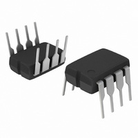
LM2574N-ADJG ON Semiconductor, LM2574N-ADJG Datasheet - Page 3

LM2574N-ADJG
Manufacturer Part Number
LM2574N-ADJG
Description
IC REG SW 0.5A ADJ OUTPUT 8-DIP
Manufacturer
ON Semiconductor
Type
Step-Down (Buck)r
Datasheet
1.LM2574N-3.3G.pdf
(26 pages)
Specifications of LM2574N-ADJG
Internal Switch(s)
Yes
Synchronous Rectifier
No
Number Of Outputs
1
Voltage - Output
1.23 ~ 37 V
Current - Output
500mA
Frequency - Switching
52kHz
Voltage - Input
4.75 ~ 40 V
Operating Temperature
-40°C ~ 125°C
Mounting Type
Through Hole
Package / Case
8-DIP (0.300", 7.62mm)
Output Voltage
1.23 V to 37 V
Output Current
0.5 A
Input Voltage
4.75 V to 40 V
Switching Frequency
52 KHz
Operating Temperature Range
- 40 C to + 125 C
Mounting Style
Through Hole
Duty Cycle (max)
98 %
Lead Free Status / RoHS Status
Lead free / RoHS Compliant
Power - Output
-
Lead Free Status / Rohs Status
Lead free / RoHS Compliant
Available stocks
Company
Part Number
Manufacturer
Quantity
Price
Company:
Part Number:
LM2574N-ADJG
Manufacturer:
ON Semiconductor
Quantity:
2 450
1. External components such as the catch diode, inductor, input and output capacitors can affect the switching regulator system performance.
2. Tested junction temperature range for the LM2574, NCV2574: T
OPERATING RATINGS
specific performance limits. For guaranteed specifications and test conditions, see the Electrical Characteristics).
SYSTEM PARAMETERS
ELECTRICAL CHARACTERISTICS
version, V
T
LM2574−3.3 ([Note 1] Test Circuit Figure 16)
LM2574−5 ([Note 1] Test Circuit Figure 16)
LM2574−12 ([Note 1] Test Circuit Figure 16)
LM2574−15 ([Note 1] Test Circuit Figure 16)
LM2574 ADJUSTABLE VERSION ([Note 1] Test Circuit Figure 16)
Operating Junction Temperature Range
Supply Voltage
Output Voltage (V
Output Voltage (4.75 V ≤ V
Efficiency (V
Output Voltage (V
Output Voltage (7.0 V ≤ V
Efficiency (V
Output Voltage (V
Output Voltage (15 V ≤ V
Efficiency (V
Output Voltage (V
Output Voltage (18 V < V
Efficiency (V
Feedback Voltage V
Feedback Voltage 7.0 V ≤ V
Efficiency (V
J
V
When the LM2574 is used as shown in the Figure 16 test circuit, the system performance will be as shown in the system parameters section
of the Electrical Characteristics.
is the operating junction temperature range that applies [Note 2], unless otherwise noted).
T
T
T
T
T
T
T
T
T
T
J
J
J
J
J
J
J
J
J
J
= 25°C
= −40 to +125°C
= 25°C
= −40 to +125°C
= 25°C
= −40 to +125°C
= 25°C
= −40 to +125°C
= 25°C
= −40 to +125°C
in
= 25 V for the 12 V version, V
in
in
in
in
in
= 12 V, I
= 12 V, I
= 15 V, I
= 18 V, I
= 12 V, I
in
in
in
in
= 12 V, I
= 12 V, I
= 25 V, I
= 30 V, I
in
= 12 V, I
Load
Load
Load
Load
Load
in
in
in
(Operating Ratings indicate conditions for which the device is intended to be functional, but do not guarantee
in
Characteristic
≤ 40 V, 0.1 A ≤ I
< 40 V, 0.1 A < I
= 0.5 A)
≤ 40 V, 0.1 A ≤ I
= 0.5 A)
= 0.5 A)
= 0.5 A)
= 0.5 A, V
in
Load
Load
Load
Load
≤ 40 V, 0.1 A ≤ I
≤ 40 V, 0.1 A ≤ I
Load
([Note 1] Test Circuit Figure 16)
= 100 mA, T
= 100 mA, T
= 100 mA, T
= 100 mA, T
Rating
= 100 mA, V
out
in
= 5.0 V)
(Unless otherwise specified, V
= 30 V for the 15 V version. I
Load
Load
Load
Load
J
J
J
J
Load
= 25°C)
= 25°C)
= 25°C)
= 25°C)
≤ 0.5 A)
out
< 0.5 A)
≤ 0.5 A)
≤ 0.5 A)
≤ 0.5 A, V
= 5.0 V, T
LM2574, NCV2574
http://onsemi.com
J
out
= 25°C
= 5.0
low
3
= −40°C T
Load
in
= 12 V for the 3.3 V, 5.0 V, and Adjustable
Symbol
= 100 mA. For typical values T
V
V
V
V
V
V
V
V
V
V
FBT
out
out
η
out
out
η
out
out
η
out
out
η
η
FB
high
Symbol
= +125°C.
V
T
in
J
3.234
3.168
3.135
11.76
11.52
14.25
1.217
1.193
4.75
14.7
14.4
1.18
11.4
Min
4.9
4.8
−
−
−
−
−
−40 to +125
1.23
1.23
Value
Typ
3.3
3.3
5.0
5.0
72
77
10
12
88
15
15
88
77
−
−
40
J
= 25°C, for min/max values
3.366
3.432
3.465
12.24
12.48
15.75
1.243
1.267
Max
5.25
12.6
15.3
15.6
1.28
5.1
5.2
−
−
−
−
−
Unit
°C
V
Unit
%
%
%
%
%
V
V
V
V
V
V
V
V
V
V


