LM2596DSADJR4G ON Semiconductor, LM2596DSADJR4G Datasheet - Page 2
LM2596DSADJR4G
Manufacturer Part Number
LM2596DSADJR4G
Description
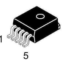
IC REG SW STP-DWN 3A D2PAK-5
Manufacturer
ON Semiconductor
Type
Step-Down (Buck)r
Datasheet
1.LM2596DSADJR4G.pdf
(25 pages)
Specifications of LM2596DSADJR4G
Internal Switch(s)
Yes
Synchronous Rectifier
No
Number Of Outputs
1
Voltage - Output
1.23 ~ 37 V
Current - Output
3A
Frequency - Switching
150kHz
Voltage - Input
4.5 ~ 40 V
Operating Temperature
-40°C ~ 125°C
Mounting Type
Surface Mount
Package / Case
D²Pak, TO-263 (5 leads + tab)
Output Voltage
1.23 V to 37 V
Output Current
3 A
Input Voltage
- 5 V to - 12 V
Switching Frequency
150 KHz
Operating Temperature Range
- 40 C to + 125 C
Mounting Style
SMD/SMT
Duty Cycle (max)
95 %
Lead Free Status / RoHS Status
Lead free / RoHS Compliant
Power - Output
-
Lead Free Status / Rohs Status
Lead free / RoHS Compliant
Available stocks
Company
Part Number
Manufacturer
Quantity
Price
Company:

Part Number:
LM2596DSADJR4G
Manufacturer:
ON
Quantity:
12 400
Part Number:
LM2596DSADJR4G
Manufacturer:
ON/安森美
Quantity:
20 000


Unregulated
Stresses exceeding Maximum Ratings may damage the device. Maximum Ratings are stress ratings only. Functional operation above the
Recommended Operating Conditions is not implied. Extended exposure to stresses above the Recommended Operating Conditions may affect
device reliability.
MAXIMUM RATINGS
Maximum Supply Voltage
ON/OFF Pin Input Voltage
Output Voltage to Ground (Steady−State)
Power Dissipation
Storage Temperature Range
Minimum ESD Rating (Human Body Model: C = 100 pF, R = 1.5 kW)
Lead Temperature (Soldering, 10 seconds)
Maximum Junction Temperature
DC Input
Case 314B and 314D (TO−220, 5−Lead)
Case 936A (D
Thermal Resistance, Junction−to−Ambient
Thermal Resistance, Junction−to−Case
Thermal Resistance, Junction−to−Ambient
Thermal Resistance, Junction−to−Case
C
in
C
FF
2
PAK)
Feedback
+V
R1
R2
1
4
in
Unregulated
DC Input
Figure 1. Typical Application and Internal Block Diagram
Band-Gap
12 V
Reference
1.235 V
Typical Application (Adjustable Output Voltage Version)
Rating
Fixed Gain
Error Amplifier
100 mF
30 kHz
Freq
Shift
C
in
Oscillator
+V
150 kHz
in
1
Comparator
3.1 V Internal
Regulator
3
http://onsemi.com
Block Diagram
LM2596
GND
5
Reset
Latch
ON/OFF
2
Current
Limit
ON/OFF
Output
Feedback
4
2
Shutdown
Thermal
Driver
D1
1N5822
33 mH
L1
3.1k
3.0 Amp
Switch
Symbol
R2
R
R
R
R
C
220 mF
T
V
P
P
T
out
qJA
qJC
qJA
qJC
−
−
stg
−
−
in
D
D
J
C
1.0k
R1
FF
ON/OFF
5
Output
2
GND
3
5.0 V Regulated
Output 3.0 A Load
−0.3 V ≤ V ≤ +V
Internally Limited
Internally Limited
−65 to +150
Value
−1.0
260
150
5.0
5.0
2.0
45
65
70
D1
L1
in
C
out
Regulated
°C/W
°C/W
°C/W
°C/W
Unit
Output
°C
kV
°C
°C
W
W
V
V
V
V
Load
out
Related parts for LM2596DSADJR4G
Image
Part Number
Description
Manufacturer
Datasheet
Request
R

Part Number:
Description:
Simple Switcher Power Converter 150 KHZ 3A Step-down Voltage Regulator, Package: to 263, Pin Nb=5
Manufacturer:
National Semiconductor

Part Number:
Description:
ON Semiconductor [VOLTAGE REGULATOR]
Manufacturer:
ON Semiconductor
Datasheet:
Part Number:
Description:
357-036-542-201 CARDEDGE 36POS DL .156 BLK LOPRO
Manufacturer:
ON Semiconductor
Datasheet:
Part Number:
Description:
357-036-542-201 CARDEDGE 36POS DL .156 BLK LOPRO
Manufacturer:
ON Semiconductor
Datasheet:
Part Number:
Description:
357-036-542-201 CARDEDGE 36POS DL .156 BLK LOPRO
Manufacturer:
ON Semiconductor
Datasheet:
Part Number:
Description:
357-036-542-201 CARDEDGE 36POS DL .156 BLK LOPRO
Manufacturer:
ON Semiconductor
Datasheet:
Part Number:
Description:
357-036-542-201 CARDEDGE 36POS DL .156 BLK LOPRO
Manufacturer:
ON Semiconductor
Datasheet:
Part Number:
Description:
357-036-542-201 CARDEDGE 36POS DL .156 BLK LOPRO
Manufacturer:
ON Semiconductor
Datasheet:
Part Number:
Description:
357-036-542-201 CARDEDGE 36POS DL .156 BLK LOPRO
Manufacturer:
ON Semiconductor
Datasheet:
Part Number:
Description:
357-036-542-201 CARDEDGE 36POS DL .156 BLK LOPRO
Manufacturer:
ON Semiconductor
Datasheet:
Part Number:
Description:
357-036-542-201 CARDEDGE 36POS DL .156 BLK LOPRO
Manufacturer:
ON Semiconductor
Datasheet:
Part Number:
Description:
357-036-542-201 CARDEDGE 36POS DL .156 BLK LOPRO
Manufacturer:
ON Semiconductor
Datasheet:
Part Number:
Description:
Manufacturer:
ON Semiconductor
Datasheet:
Part Number:
Description:
Manufacturer:
ON Semiconductor
Datasheet: