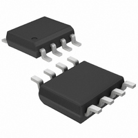
MAX1626ESA Maxim Integrated Products, MAX1626ESA Datasheet - Page 8

MAX1626ESA
Manufacturer Part Number
MAX1626ESA
Description
IC DC/DC CTRLR STEP-DWN HE 8SOIC
Manufacturer
Maxim Integrated Products
Type
Step-Down (Buck)r
Datasheet
1.MAX1627ESA.pdf
(16 pages)
Specifications of MAX1626ESA
Internal Switch(s)
No
Synchronous Rectifier
No
Number Of Outputs
1
Voltage - Output
3.3V, 5V
Current - Output
3A
Frequency - Switching
Up to 300kHz
Voltage - Input
3 ~ 16.5 V
Operating Temperature
-40°C ~ 85°C
Mounting Type
Surface Mount
Package / Case
8-SOIC (3.9mm Width)
Power - Output
471mW
Output Voltage
3.3 V, 5 V
Output Current
3 A
Input Voltage
3 V to 16.5 V
Mounting Style
SMD/SMT
Maximum Operating Temperature
+ 85 C
Minimum Operating Temperature
- 40 C
Lead Free Status / RoHS Status
Contains lead / RoHS non-compliant
Other names
Q1146982E
Available stocks
Company
Part Number
Manufacturer
Quantity
Price
Company:
Part Number:
MAX1626ESA
Manufacturer:
MAXIM
Quantity:
6
Part Number:
MAX1626ESA
Manufacturer:
MAXIM/美信
Quantity:
20 000
Company:
Part Number:
MAX1626ESA+
Manufacturer:
Maxim
Quantity:
508
Part Number:
MAX1626ESA+
Manufacturer:
MAXIM/美信
Quantity:
20 000
Company:
Part Number:
MAX1626ESA+T
Manufacturer:
MAXIM
Quantity:
12 000
Company:
Part Number:
MAX1626ESA+T
Manufacturer:
MAXIM
Quantity:
692
Part Number:
MAX1626ESA+T
Manufacturer:
MAXIM/美信
Quantity:
20 000
Part Number:
MAX1626ESA-T
Manufacturer:
MAXIM/美信
Quantity:
20 000
EXT swings from V+ to GND and provides the gate
drive for an external P-channel power MOSFET. A high-
er supply voltage increases the gate drive to the
MOSFET and reduces on-resistance (R
External Switching Transistor section.
The device’s typical quiescent current is 70µA.
However, actual applications draw additional current to
supply MOSFET switching currents, OUT pin current, or
external feedback resistors (if used), and both the diode
and capacitor leakage currents. For example, in the cir-
cuit of Figure 1, with V+ at 7V and V
no-load supply current for the entire circuit is 84µA.
When designing a circuit for high-temperature opera-
tion, select a Schottky diode with low reverse leakage.
When SHDN is high, the device enters shutdown mode.
In this mode, the feedback and control circuit, reference,
and internal biasing circuitry are turned off. EXT goes
high, turning off the external MOSFET. The shutdown
supply current drops to less than 1µA. SHDN is a logic-
level input. Connect SHDN to GND for normal operation.
The 1.3V reference is suitable for driving external loads,
such as an analog-to-digital converter. It has a guaran-
teed 10mV maximum load regulation while sourcing load
currents up to 100µA. The reference is turned off during
5V/3.3V or Adjustable, 100% Duty-Cycle,
High-Efficiency, Step-Down DC-DC Controllers
Figure 3. Discontinuous-Conduction Mode, Light-Load-Current
Waveform
8
_______________________________________________________________________________________
0A
A
B
C
CIRCUIT OF FIGURE 1, V+ = 8V, V
A: MOSFET DRAIN, 5V/div
B: OUT, 50mV/div, 5V DC OFFSET
C: INDUCTOR CURRENT, 1A/div
EXT Drive Voltage Range
10 s/div
Quiescent Current
OUT
Shutdown Mode
= 5V, LOAD = 100mA
OUT
DS(ON)
Reference
at 5V, typical
). See
shutdown. Bypass the reference with 0.1µF for normal
operation. Place the bypass capacitor within 0.2 inches
(5mm) of REF, with a direct trace to GND (Figure 7).
Soft-start reduces stress and transient voltage slumps
on the power source. When the output voltage is near
ground, the minimum off-time is lengthened to limit peak
switching current. This compensates for reduced nega-
tive inductor current slope due to low output voltages.
The MAX1626’s output voltage can be selected to 3.3V
or 5V under logic control by using the 3/5 pin. The 3/5
pin requires less than 0.5V to ensure a 3.3V output, or
more than (V+ - 0.5)V to guarantee a 5V output. The
voltage sense pin (OUT) must be connected to the out-
put for the MAX1626.
The MAX1627’s output voltage is set using two resis-
tors, R2 and R3 (Figure 5), which form a voltage divider
between the output and GND. R2 is given by:
where V
has a maximum value of 50nA, large values (10kΩ to
200kΩ) can be used for R3 with no significant accuracy
loss. For 1% error, the current through R2 should be at
Figure 4. Continuous-Conduction Mode, Heavy-Load-Current
Waveform
________________Design Information
REF
0A
A
B
C
CIRCUIT OF FIGURE 1, V+ = 8V, V
A: MOSFET DRAIN, 5V/div
B: OUT, 50mV/div, 5V DC OFFSET
C: INDUCTOR CURRENT, 1A/div
= 1.3V. Since the input bias current at FB
R2 = R3 x
Setting the Output Voltage
10 s/div
V
V
OUT
REF
OUT
1
= 5V, LOAD = 1.5A
Soft-Start


