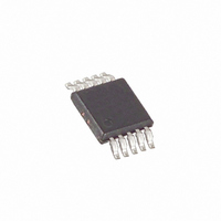
MAX1817EUB Maxim Integrated Products, MAX1817EUB Datasheet - Page 2

MAX1817EUB
Manufacturer Part Number
MAX1817EUB
Description
IC CONV DUAL DCDC STEP 10-UMAX
Manufacturer
Maxim Integrated Products
Type
Step-Up (Boost)r
Datasheet
1.MAX1817EUB.pdf
(12 pages)
Specifications of MAX1817EUB
Internal Switch(s)
Yes
Synchronous Rectifier
No
Number Of Outputs
2
Voltage - Output
3.3V or Adj Main, -28 ~ 28 V or Adj Secondary
Current - Output
125mA
Frequency - Switching
500kHz
Voltage - Input
1.5 ~ 5.5 V
Operating Temperature
-40°C ~ 85°C
Mounting Type
Surface Mount
Package / Case
10-MSOP, Micro10™, 10-uMAX, 10-uSOP
Power - Output
444mW
Lead Free Status / RoHS Status
Contains lead / RoHS non-compliant
Available stocks
Company
Part Number
Manufacturer
Quantity
Price
Company:
Part Number:
MAX1817EUB
Manufacturer:
MAXIM
Quantity:
294
Part Number:
MAX1817EUB
Manufacturer:
MAXIM/美信
Quantity:
20 000
ABSOLUTE MAXIMUM RATINGS
OUT to GND .............................................................-0.3V to +6V
ON, ONLCD, FB, FBLCD, LX to GND ......-0.3V to (V
LXLCD to GND .......................................................-0.3V to +30V
AGND to GND .......................................................-0.3V to +0.3V
Continuous Power Dissipation (T
LXLCD, LX Maximum Current ........................................0.5A
Compact, High-Efficiency, Dual-Output
Step-Up DC-DC Converter
Stresses beyond those listed under “Absolute Maximum Ratings” may cause permanent damage to the device. These are stress ratings only, and functional
operation of the device at these or any other conditions beyond those indicated in the operational sections of the specifications is not implied. Exposure to
absolute maximum rating conditions for extended periods may affect device reliability.
ELECTRICAL CHARACTERISTICS
(V
Dual Mode is a trademark of Maxim Integrated Products.
2
GENERAL
Input Voltage Range
Startup Voltage
Quiescent Current from OUT
(Main Only)
Quiescent Current from OUT
Shutdown Quiescent Current
MAIN OUTPUT
OUT Undervoltage Lockout
Fixed-Mode Output Voltage
Adjustable-Mode FB Regulation
Voltage
FB Input Bias Current
FB Dual Mode
Output Voltage Adjustment
Range
Maximum LX On-Time
Zero Crossing Comparator
Threshold (V
Zero Crossing Comparator
Backup Timer
Line Regulation
Load Regulation
LX On-Resistance
LX Current Limit
ON
10-Pin µMAX (derate 5.6mW/°C above +70°C) ...........444mW
_______________________________________________________________________________________
= V
ONLCD
PARAMETER
LX
TM
= V
- V
Threshold
OUT
OUT
)
= +3.3V, FB = GND, T
A
= +70°C)
R
R
V
V
V
V
V
V
V
V
V
V
I
V
V
I
V
OUT
LOAD
FB
ONLCD
FB
ON
OUT
OUT
FB
FB
FB
FB
IN
IN
OUT
LOAD
LOAD
= +2V to +3V
= +2.5V,
= V
= V
≤ 45mV
= 1.35V
= 0.5V
= +0.5V
= V
= 100mA,
rising, V
falling, V
= 3.3V, I
= 10mA to 100mA
= 35Ω
=
FBLCD
FBLCD
ONLCD
= 0
A
∞,
= 0°C to +85°C, unless otherwise noted. Typical values are at T
V
OUT
FB
FB
LX
FB
= 1.35V,
= 1.35V
= 0
= 1.35V
= 1.35V
= 100mA
= 1.35V
+ 0.3V)
CONDITIONS
RMS
Operating Temperature Range ...........................-40°C to +85°C
Junction Temperature ......................................................+150°C
Storage Temperature Range .............................-65°C to +150°C
Lead Temperature (soldering, 10s) .................................+300°C
1.95
3.14
1.20
MIN
1.5
2.5
2.4
0.5
45
22
0
TYP
2.15
1.25
0.35
0.75
1.5
1.2
0.1
2.2
3.3
1.6
1.6
15
75
20
45
5
5
A
= +25°C.)
MAX
1.55
3.47
1.30
0.65
1.05
105
5.5
2.4
5.5
7.5
10
30
50
40
70
1
UNITS
mV
mV
µA
µA
µA
nA
µs
µs
%
%
Ω
V
V
V
V
V
V
A


