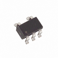
MAX1683EUK-T Maxim Integrated Products, MAX1683EUK-T Datasheet

MAX1683EUK-T
Specifications of MAX1683EUK-T
Available stocks
Related parts for MAX1683EUK-T
MAX1683EUK-T Summary of contents
Page 1
... Quiescent Current (MAX1682) ♦ Requires Only Two Capacitors ♦ 45mA Output Current PART MAX1682EUK+T -40°C to +85°C MAX1683EUK+T -40°C to +85°C Note: These parts are available in tape-and-reel only. Minimum order quantity is 2500 pieces. + Denotes a lead(Pb)-free/RoHS-compliant package Tape and reel. ...
Page 2
... Voltage Conversion Efficiency Note 3: Specifications at -40°C to +85°C are guaranteed by design. 2 _______________________________________________________________________________________ Operating Temperature Range - 0.3V MAX1682EUK/MAX1683EUK ...........................-40°C to +85°C IN Junction Temperature ......................................................+150°C Storage Temperature Range .............................-65°C to +160°C Lead Temperature (soldering, 10sec) .............................+300°C Soldering Temperature (reflow) .......................................+260°C = 0° ...
Page 3
Switched-Capacitor Voltage Doublers (Typical Operating Circuit +5V 10µF for the MAX1682 and 3.3µF for the MAX1683 noted.) OUTPUT RESISTANCE vs. SUPPLY VOLTAGE MAX1683 3.3μF 60 ...
Page 4
Switched-Capacitor Voltage Doublers (Typical Operating Circuit +5V 10µF for the MAX1682 and 3.3µF for the MAX1683 noted.) MAX1682 OSCILLATOR FREQUENCY vs. TEMPERATURE 12 12 3.3V IN ...
Page 5
Switched-Capacitor Voltage Doublers _____________________Pin Description PIN NAME FUNCTION 1 GND Ground Doubled Output Voltage. Connect C2 2 OUT between OUT and GND. Negative Terminal of the Flying 3 C1- Capacitor 4 IN Input Supply Positive Terminal of the Flying 5 ...
Page 6
Switched-Capacitor Voltage Doublers Conversion losses occur during the charge transfer between C1 and C2 when there is a voltage difference between them. The power loss is: ⎡ ⎛ ⎢ ⎜ CONVERSION LOSS ⎢ ...
Page 7
Switched-Capacitor Voltage Doublers Cascading Devices Devices can be cascaded to produce an even larger voltage (Figure 3). The unloaded output voltage is nom- inally ( where n is the number of voltage IN doublers used. ...
Page 8
Switched-Capacitor Voltage Doublers For the latest package outline information and land patterns www.maxim-ic.com/packages. Note that a “+”, “#”, or “-” in the package code indicates RoHS status only. Package drawings may show a different suffix character, but the ...
Page 9
... Maxim cannot assume responsibility for use of any circuitry other than circuitry entirely embodied in a Maxim product. No circuit patent licenses are implied. Maxim reserves the right to change the circuitry and specifications without notice at any time. 9 _____________________Maxim Integrated Products, 120 San Gabriel Drive, Sunnyvale, CA 94086 408-737-7600 © 2010 Maxim Integrated Products DESCRIPTION Maxim is a registered trademark of Maxim Integrated Products ...


