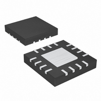
MAX5092BATE+T Maxim Integrated Products, MAX5092BATE+T Datasheet - Page 4

MAX5092BATE+T
Manufacturer Part Number
MAX5092BATE+T
Description
IC REG LDO W/BOOST 16TQFN
Manufacturer
Maxim Integrated Products
Type
Step-Up (Boost)r
Datasheet
1.MAX5092AATE.pdf
(24 pages)
Specifications of MAX5092BATE+T
Internal Switch(s)
Yes
Synchronous Rectifier
No
Number Of Outputs
2
Voltage - Output
5V, 1.5 ~ 9 V
Current - Output
250mA
Voltage - Input
3.5 ~ 72 V
Operating Temperature
-40°C ~ 125°C
Mounting Type
Surface Mount
Package / Case
16-TQFN Exposed Pad
Power - Output
2.67W
Polarity
Positive
Input Voltage Max
72 V
Output Voltage
1.5 V to 9 V, 5 V
Output Type
Adjustable, Fixed
Dropout Voltage (max)
1.6 V at 250 mA
Output Current
250 mA
Line Regulation
1.6 mV / V
Load Regulation
0.2 mV / mA
Voltage Regulation Accuracy
1.5 %
Maximum Power Dissipation
2.666 W
Maximum Operating Temperature
+ 125 C
Mounting Style
SMD/SMT
Minimum Operating Temperature
- 40 C
Reference Voltage
1.235 V
Lead Free Status / RoHS Status
Lead free / RoHS Compliant
Frequency - Switching
-
Lead Free Status / Rohs Status
Lead free / RoHS Compliant
4V to 72V Input LDOs with Boost Preregulator
ELECTRICAL CHARACTERISTICS (continued)
(V
noted. See Figures 4–7 as applicable. Typical specifications are at T
Note 2: Limits at -40°C are guaranteed by design and characterization; not production tested.
Note 3: Guaranteed minimum operating voltage is 3.5V on V
Note 4: Guaranteed by design and not production tested.
Note 5: The boost converter disable threshold (V
Note 6: The continuous maximum output current from the LDO is guaranteed according to the maximum power dissipation imposed
Note 7: Maximum output adjustable value is conditioned by the maximum adjustable BSOUT Output Voltage Range minus the maxi-
Note 8: Dropout voltage is defined as (V
4
ENABLE, HOLD and RESET
EN High Input Threshold
EN Low Input Threshold
EN Input Bias Current
HOLD Low Input Threshold
HOLD Release Voltage
HOLD Pullup Current
RESET Voltage Threshold
RESET Threshold Hysteresis
RESET Output Low Voltage
RESET Output High Leakage
Current
RESET Output Minimum Timeout
Period
EN to RESET Minimum Timeout
Delay
Delay Comparator Threshold
(Rising)
Delay Comparator Threshold
Hysteresis
CT Charge Current
CT Discharge Current
Thermal Shutdown Temperature
Threshold
Thermal Shutdown Temperature
Hysteresis
IN
_______________________________________________________________________________________
= V
EN
disable level.
by the package thermal constraints.
mum dropout across the pass transistor.
PARAMETER
= 14V, I
OUT
= 1mA, C
IN
= 47µF, C
V
SYMBOL
T
T
CTTH-HYS
I
V
V
CT-CHG
I
V
J(SHDN)
I
J(HYST)
CT-DIS
HOLD
RESET
RHYST
EN
EN
V
CTTH
I
V
I
BSOUT
V
EN
RH
RL
IH
IL
H
L
BSOUT
- V
BST_DIS
Regulator on, EN transition from high to low
EN = low
Internally connected to OUT
% of V
% of V
I
V
C
C
Temperature rising
SINK
OUT
R E S E T
CT
CT
= 22µF, C
not connected
not connected
) when V
= 1mA
OUT
OUT
) is a static measurement. Internal comparator delay may cause a higher
= 5V
, V
IN
OUT
OUT
OUT
falling only.
CONDITIONS
falling
is 2% below the value of V
= 10µF, C
A
= +25°C.) (Note 2)
VL
= 1µF, T
A
= T
OUT
J
= -40°C to +125°C, unless otherwise
V
1.205
MIN
OUT
2.4
0.4
1.5
87
for V
-
BSOUT
TYP
0.25
1.24
260
100
165
90
25
20
4
2
2
5
= V
OUT
1.265
MAX
0.4
0.4
0.4
2.5
92
2
1
+ 2V.
UNITS
mV
mA
µA
µA
µA
µA
°C
°C
µs
µs
%
%
V
V
V
V
V
V


