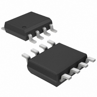
MAX1822ESA+ Maxim Integrated Products, MAX1822ESA+ Datasheet

MAX1822ESA+
Specifications of MAX1822ESA+
Related parts for MAX1822ESA+
MAX1822ESA+ Summary of contents
Page 1
... MAX1822 C2 C2- GND 4 ________________________________________________________________ Maxim Integrated Products For price, delivery, and to place orders, please contact Maxim Distribution at 1-888-629-4642, or visit Maxim’s website at www.maxim-ic.com. High-Side Power Supply ____________________________Features o +3.5V to +16.5V Operating Supply Voltage Range o Output Voltage Regulated 150µA (typ) Quiescent Current ...
Page 2
High-Side Power Supply ABSOLUTE MAXIMUM RATINGS V ......................................................................................+17V CC V ....................................................................................+30V OUT I ...................……………………………………………….25mA OUT Continuous Total Power Dissipation (T = +70°C) A 8-pin SO (derate 5.88mW/°C above +70°C)...............471mW Stresses beyond those listed under “Absolute Maximum Ratings” may cause permanent ...
Page 3
Operating Characteristics MAX1822 SUPPLY CURRENT vs. C3 CAPACITOR VALUE 400 C* = 0.01µF 350 C* = 0.033µF 300 C* = 0.022µF 250 200 150 100 C* = 0.1µ CAPACITOR VALUE (µF) ...
Page 4
High-Side Power Supply MAX1822 OUTPUT VOLTAGE RIPPLE vs. RESERVOIR CAPACITOR C3 200 T = +25°C A 180 160 V = +16.5V CC 140 I = 1mA OUT 0.01µF 120 100 ...
Page 5
INT TWO-STAGE CHARGE PUMP (SWITCHES SHOWN IN REFRESH MODE) Figure 1. MAX1822 Block Diagram Detailed Description Charge-Pump Operation The MAX1822 is a multistage charge-pump power sup- ply. Although ...
Page 6
High-Side Power Supply V SUPPLY 1000µF C1+ LOW ESR C2 0.047µ MAX1822 C2+ C2 0.047µF 2 C2- Figure 2. MAX1822 Quiescent Supply-Current Test Circuit + OUT C1+ C2 ...
Page 7
0.047µF OUT 7 C1- MAX1822 6 C2+ C2 0.047µF 2 C2- GND 4 REVERSE FORWARD Figure 4. H-Bridge Motor Controller internal switches during charge-pump cycles. This may damage the device. Output Protection ...
Page 8
High-Side Power Supply 4-CHANNEL LOAD SWITCH—NO PULLUP RESISTORS +3.5V TO +16. 1µ C1+ C1 0.01µF 7 C1- MAX1822 6 C2+ C2 0.01µF 2 C2- GND 4 NOTE 1: TRANSISTOR TYPE DEPENDS ON LOAD-CURRENT REQUIREMENTS. NOTE ...
Page 9
C5 0.1µ C1 0.01µF 7 MAX1822 C1- 6 C2+ C2 0.01µF 2 C2- GND 4 ENABLE/SHUTDOWN D2 1N914 Figure 6. Ultra-Low Dropout Positive Voltage Regulator with Logic-Controlled Enable/ Shutdown . Chip Information TRANSISTOR COUNT: 158 ...
Page 10
... Maxim cannot assume responsibility for use of any circuitry other than circuitry entirely embodied in a Maxim product. No circuit patent licenses are implied. Maxim reserves the right to change the circuitry and specifications without notice at any time. 10 ____________________Maxim Integrated Products, 120 San Gabriel Drive, Sunnyvale, CA 94086 408-737-7600 © 2001 Maxim Integrated Products Printed USA is a registered trademark of Maxim Integrated Products ...


