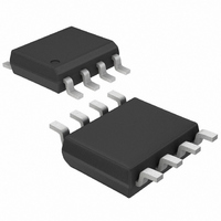
MAX1651CSA+ Maxim Integrated Products, MAX1651CSA+ Datasheet - Page 2

MAX1651CSA+
Manufacturer Part Number
MAX1651CSA+
Description
IC STP-DWN DC-DC CTRLR LDO 8SOIC
Manufacturer
Maxim Integrated Products
Type
Step-Down (Buck)r
Datasheet
1.MAX1649CSA.pdf
(12 pages)
Specifications of MAX1651CSA+
Internal Switch(s)
No
Synchronous Rectifier
No
Number Of Outputs
1
Voltage - Output
3.3V, 1.5 ~ 16 V
Current - Output
2.5A
Frequency - Switching
Up to 350kHz
Voltage - Input
3 ~ 16 V
Operating Temperature
0°C ~ 70°C
Mounting Type
Surface Mount
Package / Case
8-SOIC (3.9mm Width)
Power - Output
471mW
Output Voltage
3.3 V, 1.5 V to 16 V
Output Current
2.5 A
Input Voltage
3 V to 16 V
Mounting Style
SMD/SMT
Maximum Operating Temperature
+ 70 C
Minimum Operating Temperature
0 C
Lead Free Status / RoHS Status
Lead free / RoHS Compliant
ABSOLUTE MAXIMUM RATINGS
Supply Voltage, V+ to GND.......................................-0.3V, +17V
REF, SHDN, FB, CS, EXT, OUT .......................-0.3V, (V+ + 0.3V)
Continuous Power Dissipation (T
5V/3.3V or Adjustable, High-Efficiency,
Low-Dropout, Step-Down DC-DC Controllers
ELECTRICAL CHARACTERISTICS
(V+ = 5V, T
Stresses beyond those listed under “Absolute Maximum Ratings” may cause permanent damage to the device. These are stress ratings only, and functional
operation of the device at these or any other conditions beyond those indicated in the operational sections of the specifications is not implied. Exposure to
absolute maximum rating conditions for extended periods may affect device reliability.
2
V+ Input Voltage Range
Supply Current
FB Trip Point
FB Input Current
Output Voltage
Reference Voltage
REF Load Regulation
REF Line Regulation
Output Voltage
Line Regulation
Output Voltage
Load Regulation
Efficiency
SHDN Input Current
SHDN Input Voltage High
SHDN Input Voltage Low
Plastic DIP (derate 9.09mW/°C above +70°C) .............727mW
SO (derate 5.88mW/°C above +70°C) ..........................471mW
_______________________________________________________________________________________
PARAMETER
A
= T
MIN
to T
MAX
SYMBOL
, unless otherwise noted. Typical values are at T
V
V
V
I
V
OUT
V+
REF
I+
FB
IH
IL
A
= +70°C)
V
V+ = 16V, SHDN ≤ 0.4V (operating, switch off)
V+ = 16V, SHDN ≥ 1.6V (shutdown)
V+ = 10V, SHDN ≥ 1.6V (shutdown)
MAX1649C, MAX1651C
MAX1649E, MAX1651E
MAX1649C, MAX1651C
MAX1649E, MAX1651E
MAX1649, V+ = 5.5V to 16V
MAX1651, V+ = 3.6V to 16V
MAX1649C, MAX1651C, I
MAX1649E, MAX1651E, I
0µA ≤ I
3V ≤ V+ ≤ 16V
Circuit of
Figure 1
Circuit of
Figure 1
Circuit of
Figure 1
V+ = 16V, SHDN = 0V or V+
3V ≤ V+ ≤ 16V
3V ≤ V+ ≤ 16V
OUT
< V+
REF
≤ 100µA, sourcing only
CONDITIONS
MAX1649, 5.5V ≤ V+ ≤ 16V,
I
MAX1651, 3.6V ≤ V+ ≤ 16V,
I
MAX1649, 0A ≤ I
V
MAX1651, 0A ≤ I
V
MAX1649, V+ = 10V,
I
MAX1651, V+ = 5V,
I
LOAD
LOAD
LOAD
LOAD
REF
IN
IN
REF
= 10V
= 5V
= 0μA
= 0μA
Operating Temperature Ranges
Storage Temperature Range .............................-65°C to +160°C
Lead Temperature (soldering, 10sec) .............................+300°C
= 1A
= 1A
= 1A
= 1A
MAX1649C_A, MAX1651C_A ..............................0°C to +70°C
MAX1649E_A, MAX1651E_A ............................-40°C to +85°C
A
= +25°C.)
LOAD
LOAD
≤ 1.5A,
≤ 1.5A,
1.4625
1.4625
1.470
1.470
4.80
3.17
MIN
3.0
1.6
TYP
-47
-45
1.5
1.5
5.0
3.3
1.5
1.5
2.6
1.7
78
40
90
90
2
1
4
1.5375
1.5375
1.530
1.530
MAX
5.20
3.43
±50
±70
100
100
0.4
16
10
5
1
UNITS
mV/A
mV/V
µV/V
mV
µA
nA
µA
%
V
V
V
V
V
V


