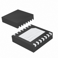
MAX8625AETD+T Maxim Integrated Products, MAX8625AETD+T Datasheet - Page 3

MAX8625AETD+T
Manufacturer Part Number
MAX8625AETD+T
Description
IC PWM STEP-UP/DWN REG 14-TDFN
Manufacturer
Maxim Integrated Products
Type
Step-Down (Buck), Step-Up (Boost)r
Datasheet
1.MAX8625AETDT.pdf
(16 pages)
Specifications of MAX8625AETD+T
Internal Switch(s)
Yes
Synchronous Rectifier
Yes
Number Of Outputs
1
Voltage - Output
3.3V, 1.25 ~ 4 V
Current - Output
800mA
Frequency - Switching
1MHz
Voltage - Input
2.5 ~ 5.5 V
Operating Temperature
-40°C ~ 85°C
Mounting Type
Surface Mount
Package / Case
14-TDFN Exposed Pad
Power - Output
1.48W
Lead Free Status / RoHS Status
Lead free / RoHS Compliant
ELECTRICAL CHARACTERISTICS (continued)
(V
Typical values are at T
Note 2: The device is production tested at T
Note 3: Limits are guaranteed by design and not production tested.
Note 4: The idle-mode current threshold is the transition point between fixed-frequency PWM operation and idle-mode operation.
FB Dual-Mode Threshold
FB Leakage Current
ON, SKIP Input High Voltage
ON, SKIP Input Low Voltage
ON Input Leakage Current
SKIP Input Leakage Current
Peak Current Limit
Fault Latch-Off Delay
MOSFET On-Resistance
Rectifier-Off Current Threshold
Idle-Mode Current Threshold
(Note 4)
LX1, LX2 Leakage Current
Out Reverse Current
Minimum T
OSC Frequency
Thermal Shutdown
IN
= 3.6V, ON = SKIP = IN, FB = GND, V
design and characterization.
The specification is given in terms of output load current for an inductor value of 3.3µH. For the step-up mode, the idle-mode
transition varies with input to the output-voltage ratios.
PARAMETER
ON
_______________________________________________________________________________________
A
= +25°C, unless otherwise noted.) (Note 2)
High-Efficiency, Seamless Transition,
F
SYMBOL
I
I
T
OSCPWM
V
LXLKGR
I
I
LX1OFF
I
LXLKG
SKIPH
I
ONMIN
SKIPL
I
R
FBDM
LIMP
I
SKIP
V
I
V
IHL
FB
ON
IH
IL
OUT
A
Step-Up/Down DC-DC Converter
= +25°C. Specifications over the operating temperature range are guaranteed by
= 3.3V, LX_ unconnected, C
V
V
2.5V < V
2.5V < V
2.5V < V
T
V
V
LX1 PMOS
Each MOSFET, T
Each MOSFET, V
T
SKIP = GND
SKIP = GND, load decreasing
Load increasing
V
V
T
V
measure I (LX2), T
T
15°C hysteresis
A
A
A
A
FB
FB
SKIP
SKIP
IN
LX2
IN
= +85°C
= -40°C to +85°C
= +85°C
= +85°C
= V
= V
= 1.3V, T
= 1.3V, T
= 0V to V
= 3.6V
= 0V
OUT
LX1
IN
IN
IN
< 5.5V
< 5.5V
< 5.5V, T
= V
= 5.5V, V
A
A
OUT
LX2
CONDITIONS
= +25°C
= +85°C
A
IN
, T
A
= 0V, V
= +25°C
= 2.5V to 5.5V,
A
= +25°C
A
LX1
= +25°C
= +25°C
= 0V to V
OUT
REF
= C5 = 0.1µF to GND, Figure 4. T
= 5.5V,
IN
,
1700
MIN
850
1.6
75
-2
0.001
0.001
+165
2000
1000
TYP
0.01
0.01
0.05
0.01
0.01
-0.2
100
100
125
100
300
0.2
0.5
25
3
A
= -40°C to +85°C.
MAX
2300
1150
0.45
125
0.1
0.1
0.2
12
1
1
1
UNITS
kHz
mV
mA
mA
mA
ms
µA
µA
µA
µA
µA
°C
%
Ω
V
V
3


