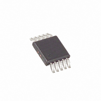
MAX1745EUB+T Maxim Integrated Products, MAX1745EUB+T Datasheet - Page 10

MAX1745EUB+T
Manufacturer Part Number
MAX1745EUB+T
Description
IC DC-DC CNTRLR STP DWN 10UMAX
Manufacturer
Maxim Integrated Products
Type
Step-Down (Buck)r
Datasheet
1.MAX1744EUB.pdf
(15 pages)
Specifications of MAX1745EUB+T
Internal Switch(s)
No
Synchronous Rectifier
No
Number Of Outputs
1
Voltage - Output
1.25 ~ 18 V
Frequency - Switching
330kHz
Voltage - Input
4.5 ~ 36 V
Operating Temperature
-40°C ~ 85°C
Mounting Type
Surface Mount
Package / Case
10-MSOP, Micro10™, 10-uMAX, 10-uSOP
Power - Output
444mW
Output Voltage
1.25 V to 18 V
Output Current
10 A
Input Voltage
4.5 V to 36 V
Mounting Style
SMD/SMT
Maximum Operating Temperature
+ 85 C
Minimum Operating Temperature
- 40 C
Lead Free Status / RoHS Status
Lead free / RoHS Compliant
Current - Output
-
Lead Free Status / Rohs Status
Lead free / RoHS Compliant
High-Voltage, Step-Down DC-DC
Controllers in µMAX
Figure 3. Discontinuous-Conduction Mode, Light-Load-Current
Waveform
The MAX1744/MAX1745 contain a 5V low-side linear reg-
ulator (VL) that powers the internal circuit and can supply
up to 1mA to an external load. This allows the
MAX1744/MAX1745 to operate up to 36V input, while
maintaining low quiescent current and high switching fre-
quency. When the input voltage goes below 5.5V, this
regulator goes into dropout and the IN pin quiescent cur-
rent will rise. See the Typical Operating Characteristics .
Bypass VL with a 4.7μF or greater capacitor.
The MAX1744/MAX1745 contain a high-side linear regu-
lator (VH) that regulates its output to 5V below IN (the
positive supply input voltage). This regulator limits the
external P-channel MOSFET gate swing (EXT), allowing
high input voltage operation without exceeding the
MOSFET gate-source breakdown. Bypass VH with a
4.7μF or greater capacitor between IN and VH. Fast line
transients may drive the voltage on VH negative. The
clamp diode (D2) prevents damage to the IC during
such a condition. A Schottky diode with a minimum 40V
reverse rating such as the Nihon EP05Q04 is sufficient
for most applications.
The devices’ typical quiescent current is 90μA.
However, actual applications draw additional current to
supply MOSFET switching currents, OUT pin current,
external feedback resistors (if used), and both the diode
and capacitor leakage currents. For example, in the cir-
cuit of Figure 1, with IN at 30V and V
no-load supply current for the entire circuit is 100μA.
10
______________________________________________________________________________________
CIRCUIT OF FIGURE 1, V
A: MOSFET DRAIN, 10V/div
B: OUT, 50mV/div, 3.3V DC OFFSET
C: INDUCTOR CURRENT, 1A/div
A
C
B
IN
10μs/div
= 18V, V
VH Linear Regulator
VL Linear Regulator
Quiescent Current
OUT
= 3.3V, I
OUT
LOAD
at 5V, typical
= 100mA
When SHDN is low, the device enters shutdown mode. In
this mode, the internal circuitry is turned off. EXT is pulled
to IN, turning off the external MOSFET. The shutdown
supply current drops to less than 10μA. SHDN is a logic-
level input. Connect SHDN to IN for normal operation.
The 1.25V reference is suitable for driving small external
loads. It has a guaranteed 10mV maximum load regula-
tion while sourcing load currents up to 100μA. The refer-
ence is turned off during shutdown. Bypass the
reference with 0.1μF for normal operation. Place the
bypass capacitor within 0.2in (5mm) of REF, with a direct
trace to GND.
The MAX1744’s output voltage can be selected to 3.3V
or 5V under logic control by using the 3/5 pin. Connect
the 3/5 pin to GND to ensure a 3.3V output, or connect
the 3/5 pin to V
The MAX1745’s output voltage is set using two resis-
tors, R2 and R3 (Figure 5), which form a voltage-divider
between the output and FB. R2 is given by:
where V
has a maximum value of 50nA, large values (10kΩ to
200kΩ) can be used for R3 with no significant accuracy
Figure 4. Continuous-Conduction Mode, Heavy-Load-Current
Waveform
REF
CIRCUIT OF FIGURE 1, V
A: MOSFET DRAIN, 10V/div
B: OUT, 50mV/div, 3.3V DC OFFSET
C: INDUCTOR CURRENT, 1A/div
= 1.25V. Since the input bias current at FB
C
A
B
L
R2= R3 x
to ensure a 5V output.
Setting the Output Voltage
Design Information
IN
⎛
⎜
⎝
10μs/div
= 18V, V
V
V
OUT
REF
OUT
Shutdown Mode
−
= 3.3V, I
⎟ 1
⎞
⎠
LOAD
Reference
= 1.5A


