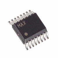
MAX1763EEE Maxim Integrated Products, MAX1763EEE Datasheet - Page 4

MAX1763EEE
Manufacturer Part Number
MAX1763EEE
Description
IC CONV DC/DC STEP UP LN 16QSOP
Manufacturer
Maxim Integrated Products
Type
Step-Up (Boost)r
Datasheet
1.MAX1763EEE.pdf
(16 pages)
Specifications of MAX1763EEE
Internal Switch(s)
Yes
Synchronous Rectifier
Yes
Number Of Outputs
1
Voltage - Output
3.3V, 2.5 ~ 5.5 V
Current - Output
1.5A
Frequency - Switching
1MHz
Voltage - Input
0.7 ~ 5.5 V
Operating Temperature
-40°C ~ 85°C
Mounting Type
Surface Mount
Package / Case
16-QSOP
Power - Output
667mW
Output Voltage
3.3 V
Output Current
1.5 A
Input Voltage
0.7 V to 5.5 V
Supply Current
2.5 mA
Switching Frequency
1200 MHz
Mounting Style
SMD/SMT
Maximum Operating Temperature
+ 85 C
Minimum Operating Temperature
- 40 C
Lead Free Status / RoHS Status
Contains lead / RoHS non-compliant
Available stocks
Company
Part Number
Manufacturer
Quantity
Price
Part Number:
MAX1763EEE
Manufacturer:
MAXIM/美信
Quantity:
20 000
1.5A, Low-Noise, 1MHz, Step-Up
DC-DC Converter
ELECTRICAL CHARACTERISTICS
(CLK/SEL = ONB = FB = PGND = GND, ISET = REF, OUT = POUT, V
wise noted.) (Note 8)
4
DC-DC CONVERTER
Input Voltage Range (Note 1)
M i ni m um S tartup V ol tag e ( N ote 2)
Frequency in Startup Mode
Internal Oscillator Frequency
Oscillator Maximum Duty Cycle
(Note 3)
E xter nal C l ock Fr eq uency Rang e
Output Voltage
FB Regulation Voltage
FB Input Current
Output Voltage Adjust Range
Output Voltage Lockout
Threshold (Note 4)
ISET Input Leakage Current
Supply Current in Shutdown
No-Load Supply Current, Low-
Power Mode (Note 5)
Gain Block Supply Current
DC-DC SWITCHES
POUT Leakage Current
LX Leakage Current
Switch On-Resistance
N-Channel Current Limit
P-Channel Turn-Off Current
REFERENCE
Reference Output Voltage
Reference Load Regulation
Reference Supply Rejection
GAIN BLOCK
AIN Reference Voltage
AIN Input Current
Transconductance
AO Output Low Voltage
AO Output High Leakage
_______________________________________________________________________________________
PARAMETER
I
V
CLK/SEL = OUT
V
for 0 < I
Adjustable output, CLK/SEL = OUT, includes load
regulation for 0 < I
V
Rising edge
V
V
CLK/SEL = GND, AIN = OUT
V
V
V
N-channel
P-channel
CLK/SEL = GND
I
-1µA < I
2.5V < V
I
V
V
V
V
LOAD
REF
AO
OUT
FB
FB
ISET
AIN
LX
LX
AIN
AO
AIN
AIN
ONB
= V
= 20µA
= 0, V
< 0.1V, CLK/SEL = OUT, includes load regulation
= 1.35V
= 0
= 1V, 10µA < I
= 1.5V
= 0.5V, I
< (V
= 1.5V, V
= 1.25V
< 1mA, T
= 1.5V
= 3.6V, V
ONB
LX
REF
OUT
OUT
OUT
< 1.1A
< 50µA
= V
< 5V
AO
- 1.4V), gain block enabled
AO
= 5.5V
A
ONA
OUT
= 100µA
= +25°C
= 5.5V
LX
AO
= 5.5V, V
= 0
< 1.1A
CONDITIONS
< 100µA
ONA
ONA
= 0
= V
AIN
= V
OUT
= 3.6V, T
1.215
1.220
0.75
3.17
2.00
MIN
125
910
0.6
2.5
2.0
80
10
A
5
= -40°C to +85°C, unless other-
1.270
1.270
MAX
1000
1.25
3.38
2.30
0.13
0.25
±30
100
200
240
970
5.5
1.1
1.2
5.5
3.4
0.4
91
50
10
50
10
10
15
16
5
1
UNITS
MHz
MHz
kHz
mA
mV
mV
mV
mS
nA
nA
µA
µA
µA
µA
µA
nA
µA
%
Ω
V
V
V
V
V
V
A
V
V


