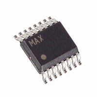
MAX1677EEE Maxim Integrated Products, MAX1677EEE Datasheet - Page 12

MAX1677EEE
Manufacturer Part Number
MAX1677EEE
Description
IC CONV DC-DC STEP-UP 16-QSOP
Manufacturer
Maxim Integrated Products
Type
Step-Up (Boost)r
Datasheet
1.MAX1677EEE.pdf
(16 pages)
Specifications of MAX1677EEE
Internal Switch(s)
Yes
Synchronous Rectifier
Yes
Number Of Outputs
2
Voltage - Output
3.3V or Adj Main, -28 ~ 28 V or Adj Secondary
Current - Output
350mA
Frequency - Switching
300kHz
Voltage - Input
0.7 ~ 5.5 V
Operating Temperature
-40°C ~ 85°C
Mounting Type
Surface Mount
Package / Case
16-QSOP
Power - Output
696mW
Output Voltage
2.5 V to 5.5 V
Output Current
350 mA
Input Voltage
0.7 V to 5.5 V
Supply Current
35 uA
Switching Frequency
300 KHz
Mounting Style
SMD/SMT
Maximum Operating Temperature
+ 85 C
Minimum Operating Temperature
- 40 C
Lead Free Status / RoHS Status
Contains lead / RoHS non-compliant
Available stocks
Company
Part Number
Manufacturer
Quantity
Price
Company:
Part Number:
MAX1677EEE
Manufacturer:
MAXIM
Quantity:
247
Part Number:
MAX1677EEE
Manufacturer:
MAXIM/美信
Quantity:
20 000
Part Number:
MAX1677EEE+
Manufacturer:
MAXIM/美信
Quantity:
20 000
off time reduces transient input current when the LCD is
activated.
A logic-low level at ON shuts down all MAX1677 cir-
cuits including the LCD converter, reference, and LBI
comparator. A logic-high level at LCDON activates the
LCD boost converter. The LCD boost converter can
only be activated when ON is high. When ON is low,
the MAX1677 draws 1µA.
The MAX1677 has an on-chip comparator for low-bat-
tery detection. If the voltage at LBI falls below 614mV,
LBO (an open-drain output) sinks current to GND. The
low-battery trip level is set by two resistors (Figure 6).
Since the LBI input current is less than 50nA, large
resistor values (R6 ≤ 130kΩ) can be used to minimize
input loading. Calculate R5 as follows:
Connect a pullup resistor (R8) to LBO when driving
CMOS logic. LBO is an open-drain output and can be
pulled as high as 6V regardless of the voltage at OUT.
When LBI is above 0.614V, LBO is high impedance. If
the LBI comparator is not used, ground LBI.
Since the low-battery comparator is noninverting, hys-
teresis can be added by connecting a resistor (R7)
from LBI to LBO as shown in Figure 7. When LBO is
Compact, High-Efficiency, Dual-Output
Step-Up and LCD Bias DC-DC Converter
Table 3. Setting LCD Output Polarity and
Peak Inductor Current
Figure 6. Setting the Low-Battery Trip Threshold
12
POLARITY
OUTPUT
Negative
Negative
Positive
Positive
R5
R6
V
IN
LCD
______________________________________________________________________________________
(V
TRIP
)
LBI
R5 = R6 [(V
GND through 50kΩ
CONNECTED TO:
OUT through 50kΩ
MAX1677
LCDPOL
GND
OUT
Shutdown: ON and LCDON
Low-Battery Comparator
POUT
LBO
TRIP
/ 0.614V) - 1]
INDUCTOR CURRENT
R8
L
CDLX
LOGIC POWER
LOW-BATTERY OUTPUT
(mA)
350
350
225
225
PEAK
high, the series combination of R8 and R7 source cur-
rent into the summing node at LBI (no current flows into
the IC).
The MBC feedback pin (FB) features Dual Mode opera-
tion. With FB grounded, the MBC output is preset to
3.3V. It can also be adjusted from 2.5V to 5.5V with
external resistors, R3 and R4, as shown in Figure 8. To
set the output voltage externally, select resistor R4 in
the 10kΩ to 200kΩ range. Calculate R3 using:
For either positive or negative LCD output voltages, set
the voltage with two external resistors, R1 and R2, as
shown in Figures 2 and 3. Since the input current at FB
has a maximum of 50nA, large resistors can be used
without significant accuracy loss. Begin by selecting R2
Figure 7. Adding External Hysteresis to the LBI Comparator
Figure 8. Setting the MBC Output Voltage Externally
V
V
WHERE V
AND V
IN
H
R5
R6
= 0.614V
(V
TRIP
L
IS THE FALLING V
: V
H
IS THE RISING V
H
[
1 + R5 + R5
, V
L
R7 R6
)
MAX1677
R3 = R4 [(V
Setting the LCD Output Voltage
LBI
]
TRIP
TRIP
MAX1677
POUT
LEVEL.
GND
R7
LEVEL
FB
V
L
OUT
= 0.614V + R5
Design Procedure
POUT
LBO
/ 1.25V) - 1]
R3
R4
(
0.614V
R6
R8
100k
MBC OUTPUT
-
(
V
POUT
R7 + R8
- 0.614V
)
)


