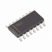
MAX797CSE Maxim Integrated Products, MAX797CSE Datasheet - Page 21

MAX797CSE
Manufacturer Part Number
MAX797CSE
Description
IC CONTRLR STEP-DOWN PWM 16-SOIC
Manufacturer
Maxim Integrated Products
Type
Step-Down (Buck)r
Datasheet
1.MAX797CSE.pdf
(32 pages)
Specifications of MAX797CSE
Internal Switch(s)
No
Synchronous Rectifier
Yes
Number Of Outputs
2
Voltage - Output
3.3V, 5V, Adj
Current - Output
10A
Frequency - Switching
150kHz, 300kHz
Voltage - Input
4.5 ~ 30 V
Operating Temperature
0°C ~ 70°C
Mounting Type
Surface Mount
Package / Case
16-SOIC (3.9mm Width)
Power - Output
696mW
Output Voltage
5 V
Output Current
10 A
Switching Frequency
340 KHz
Maximum Operating Temperature
+ 70 C
Mounting Style
SMD/SMT
Minimum Operating Temperature
0 C
Supply Current
0.44 mA
Case
sop
Dc
99+
Lead Free Status / RoHS Status
Contains lead / RoHS non-compliant
Available stocks
Company
Part Number
Manufacturer
Quantity
Price
Company:
Part Number:
MAX797CSE
Manufacturer:
MAXIM
Quantity:
9 800
Part Number:
MAX797CSE
Manufacturer:
MAXIM/美信
Quantity:
20 000
Company:
Part Number:
MAX797CSE+
Manufacturer:
Maxim
Quantity:
300
Company:
Part Number:
MAX797CSE+T
Manufacturer:
MAXIM
Quantity:
3
Company:
Part Number:
MAX797CSE-T
Manufacturer:
SP
Quantity:
226
Part Number:
MAX797CSE-T
Manufacturer:
MAXIM/美信
Quantity:
20 000
These equations are “worst-case” with 45 degrees of
phase margin to ensure jitter-free fixed-frequency opera-
tion and provide a nicely damped output response for
zero to full-load step changes. Some cost-conscious
designers may wish to bend these rules by using less
expensive (lower quality) capacitors, particularly if the
load lacks large step changes. This practice is tolerable,
provided that some bench testing over temperature is
done to verify acceptable noise and transient response.
There is no well-defined boundary between stable and
unstable operation. As phase margin is reduced, the
first symptom is a bit of timing jitter, which shows up as
blurred edges in the switching waveforms where the
scope won’t quite sync up. Technically speaking, this
(usually) harmless jitter is unstable operation, since the
switching frequency is now non-constant. As the
capacitor quality is reduced, the jitter becomes more
pronounced and the load-transient output voltage
waveform starts looking ragged at the edges.
Eventually, the load-transient waveform has enough
ringing on it that the peak noise levels exceed the
allowable output voltage tolerance. Note that even with
zero phase margin and gross instability present, the
output voltage noise never gets much worse than I
x R
Designers of RF communicators or other noise-sensi-
tive analog equipment should be conservative and
stick to the guidelines. Designers of notebook comput-
ers and similar commercial-temperature-range digital
systems can multiply the R
without hurting stability or transient response.
The output voltage ripple is usually dominated by the
ESR of the filter capacitor and can be approximated as
I
full equation for ripple in the continuous mode is
V
idle mode, the inductor current becomes discontinuous
with high peaks and widely spaced pulses, so the
noise can actually be higher at light load compared to
full load. In idle mode, the output ripple can be calcu-
lated as:
RIPPLE
NOISE(p-p)
ESR
———————————————————
(under constant loads, at least).
0.0003 x L x [1 / V
x R
ESR
V
= I
NOISE(p-p)
. There is also a capacitive term, so the
RIPPLE
______________________________________________________________________________________
(R
x (R
SENSE
= —————— +
Synchronous Rectifier for CPU Power
OUT
ESR
ESR
0.02 x R
)
2
+ 1 / (V
R
+ 1 / (2 x pi x f x C
x C
SENSE
value by a factor of 1.5
F
ESR
IN
- V
OUT
)]
Step-Down Controllers with
F
PEAK
)). In
Buck-plus-flyback applications, sometimes called “cou-
pled-inductor” topologies, need a transformer in order to
generate multiple output voltages. The basic electrical
design is a simple task of calculating turns ratios and
adding the power delivered to the secondary in order to
calculate the current-sense resistor and primary induc-
tance. However, extremes of low input-output differen-
tials, widely different output loading levels, and high turns
ratios can complicate the design due to parasitic trans-
former parameters such as inter-winding capacitance,
secondary resistance, and leakage inductance. For
examples of what is possible with real-world transformers,
see the graphs of Maximum Secondary Current vs. Input
Voltage in the Typical Operating Characteristics.
Power from the main and secondary outputs is lumped
together to obtain an equivalent current referred to the
main output voltage (see Inductor L1 for definitions of
parameters). Set the value of the current-sense resistor
at 80mV / I
P
I
where: V
In positive-output (MAX796) applications, the trans-
former secondary return is often referred to the main
output voltage rather than to ground in order to reduce
the needed turns ratio. In this case, the main output
voltage must first be subtracted from the secondary
voltage to obtain V
TOTAL
TOTAL
Turns Ratio N = ——————————————
L(primary) = —————————————
= P
ondary-output voltage
rectifier
output voltage (from the Electrical
Characteristics)
synchronous-rectifier MOSFET
resistor
V
V
V
V
= the sum of the output power from all outputs
SEC
FWD
OUT(MIN)
RECT
SENSE
TOTAL
rent referred to V
TOTAL
is the minimum required rectified sec-
is the forward drop across the secondary
is the on-state voltage drop across the
is the voltage drop across the sense
.
SEC
is the minimum value of the main
/ V
V
OUT
V
.
OUT(MIN)
V
IN(MAX)
OUT
(MAX796/MAX799 Only)
= the equivalent output cur-
V
OUT
SEC
(V
Transformer Design
IN(MAX)
x f x I
+ V
+ V
RECT
FWD
TOTAL
- V
+ V
OUT
x LIR
SENSE
)
21


