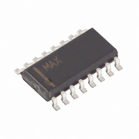
MAX1709ESE Maxim Integrated Products, MAX1709ESE Datasheet - Page 11

MAX1709ESE
Manufacturer Part Number
MAX1709ESE
Description
IC DC/DC CONV STEP-UP 4A 16-SOIC
Manufacturer
Maxim Integrated Products
Type
Step-Up (Boost)r
Datasheet
1.MAX1709ESE.pdf
(15 pages)
Specifications of MAX1709ESE
Internal Switch(s)
Yes
Synchronous Rectifier
No
Number Of Outputs
1
Voltage - Output
3.3V, 5V, Adj
Current - Output
4A
Frequency - Switching
600kHz
Voltage - Input
0.7 ~ 5 V
Operating Temperature
-40°C ~ 85°C
Mounting Type
Surface Mount
Package / Case
16-SOIC (3.9mm Width)
Power - Output
1.3W
Lead Free Status / RoHS Status
Contains lead / RoHS non-compliant
Other names
Q1226679
Available stocks
Company
Part Number
Manufacturer
Quantity
Price
Company:
Part Number:
MAX1709ESE
Manufacturer:
MAXIM
Quantity:
19
Company:
Part Number:
MAX1709ESE
Manufacturer:
MAXIM
Quantity:
106
Part Number:
MAX1709ESE+
Manufacturer:
MAXIM/美信
Quantity:
20 000
Figure 5. Momentary Pushbutton On-Off Switch
V
current
V
D' = (V
is negligible
f = switching frequency
L1 = inductor value
I
trical Characteristics or set by R
The MAX1709’s high switching frequency demands a
high-speed rectifier. Schottky diodes, such as the
MBRD1035CTL or STPS8L30B (Table 3), are recom-
mended. The diode’s current rating must exceed the
maximum load current, and its breakdown voltage must
exceed V
of the LX switching node and the output filter capacitor.
The diode also must be able to dissipate the power cal-
culated by the following equation:
where I
diode forward voltage at the peak switch current.
Two 150µF, low-ESR tantalum input capacitors will
reduce peak currents and reflected noise due to induc-
tor current ripple. Lower ESR allows for lower input rip-
ple current, but combined ESR values up to 50mΩ are
acceptable. Smaller ceramic capacitors may also be
used for light loads or in applications that can tolerate
higher input current ripple.
LIM
D
OUT
= forward voltage drop of the Schottky diode at I
= minimum value of switch current limit from Elec-
= output voltage
IN
ON/OFF
OUT
) / (V
OUT
is the average load current and V
0.1μF
OUT
. The diode must be placed within 10mm
270k
P
______________________________________________________________________________________
+ V
DIODE
Input Bypass Capacitors (C1, C2)
D
), assuming switch voltage drop
ONB
ONA
MAX1709
= I
OUT
Diode Selection (D1)
Capacitor Selection
270k
SET/LIM
V
D
.
4A, Low-Noise, High-Frequency,
V
I/O
I/O
DD
μC
D
is the
LIM
Step-Up DC-DC Converter
The output filter capacitor ESR must be kept under
15mΩ for stable operation. Two parallel 150µF polymer
capacitors (Panasonic EEFUE0J151R) typically exhibit
5mΩ of ESR. This translates to approximately 35mV of
output ripple at 7A switch current. Bypass the
MAX1709 IC supply input (OUT) with a 0.1µF ceramic
capacitor to GND and connect a 2Ω series resistor to
OUT (R2, as shown in Figure 1).
The MAX1709 output current may be more limited by
package power dissipation than by the current rating of
the on-chip switch. For pulsed loads, output currents of
4 Amps or more can be supplied with either the
MAX1709EUI+ or MAX1709ESE, but the RMS (or ther-
mal) limit of the MAX1709ESE is lower (6A
that of the MAX1709EUI+ (10A
current depends on the input and output voltage, oper-
ating temperature, and external components.
The major components of the MAX1709 dissipated
power (P
NOT delivered to the load) are:
These are losses that directly dissipate heat in the
MAX1709, but keep in mind that other losses, such as
those in the external diode and inductor, increase input
power by reducing overall efficiency, and so indirectly
contribute to MAX1709 heating.
Approximate equations for the loss terms are as fol-
lows. Values in {} are example values for a 3.3V input,
4V output, 4A design.
A conservative efficiency estimate for the MAX1709
boosting from 3.3V to 5V at 4A is 81%. Total estimated
power loss is then:
The total loss consists of:
1) Internal switch conduction losses - P
2) Internal switch transition losses - P
3) Internal capacitive losses - P
P
Diode Loss = D’ x I
Inductor Loss (resistive loss + dynamic loss
External Capacitive Loss = (1 - D’) x I
MAX1709 Internal Loss, P
LOSS
estimate)
R
CAP-ESR
D
= (P
, i.e., power dissipated as heat in the IC and
OUT
(ESR est. = 10mΩ)
/ 0.81) - P
Output Filter Capacitors (C6, C7)
SW
x V
OUT
D(MAX1709)
D
RMS
Power Dissipation
CAP
). Continuous output
TRAN
SW
SW
2
x
RMS
{0.58W}
{0.27W}
{1.35W}
{4.7W}
{2.5W}
) than
11


