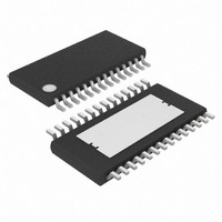
MAX1945SEUI+T Maxim Integrated Products, MAX1945SEUI+T Datasheet - Page 2

MAX1945SEUI+T
Manufacturer Part Number
MAX1945SEUI+T
Description
IC REG STP DWN 6A 28-TSSOP
Manufacturer
Maxim Integrated Products
Type
Step-Down (Buck)r
Datasheet
1.MAX1945REUI.pdf
(19 pages)
Specifications of MAX1945SEUI+T
Internal Switch(s)
Yes
Synchronous Rectifier
No
Number Of Outputs
1
Voltage - Output
1.8V, 2.5V, Adj
Current - Output
6A
Frequency - Switching
1MHz
Voltage - Input
2.6 ~ 5.5 V
Operating Temperature
-40°C ~ 85°C
Mounting Type
Surface Mount
Package / Case
28-TSSOP Exposed Pad, 28-eTSSOP, 28-HTSSOP
Power - Output
1.19W
Lead Free Status / RoHS Status
Lead free / RoHS Compliant
ABSOLUTE MAXIMUM RATINGS
CTL1, CTL2, IN, SYNC, V
SYNCOUT, COMP, FB, FBSEL,
LX Current (Note 1) .....................................................-9A to +9A
BST to LX..................................................................-0.3V to +6V
PGND to GND .......................................................-0.3V to +0.3V
ELECTRICAL CHARACTERISTICS
(V
otherwise noted. Typical values are at +25°C.)
1MHz, 1% Accurate, 6A Internal Switch
Step-Down Regulators
Stresses beyond those listed under “Absolute Maximum Ratings” may cause permanent damage to the device. These are stress ratings only, and functional
operation of the device at these or any other conditions beyond those indicated in the operational sections of the specifications is not implied. Exposure to
absolute maximum rating conditions for extended periods may affect device reliability.
Note 1:
2
IN/V
Input Voltage
IN Supply Current
V
V
Total Shutdown Current from IN,
V
V
Threshold
V
V
BST
BST Shutdown Supply Current
REF
REF Voltage
REF Shutdown Resistance
COMP
COMP Transconductance
COMP Clamp Voltage Low
COMP Clamp Voltage High
COMP Shutdown Resistance
IN
REF to GND ............................................-0.3V to (V
CC
DD
CC
CC
DD
DD
_______________________________________________________________________________________
= V
, and V
CC
Shutdown Supply Current
Supply Current
Supply Current
Undervoltage Lockout
CC
LX has internal clamp diodes to PGND and IN. Applications that forward bias these diodes should take care not to exceed
the IC’s package power dissipation limits.
PARAMETER
= V
DD
CTL1
= V
CTL2
CC
, V
= V
DD
DD
to GND ...............-0.3V to +6V
= 3.3V, SYNC = GND, FBSEL = High-Z, V
SYMBOL
V
I
V
V
CLAMP
CLAMP
TOTAL
V
HIGH_
I
UVLO
LOW_
I
I
V
BST
I
CC
DD
REF
IN
IN
SYNC = V
no load
SYNC = V
SYNC = V
V
CTL1 = CTL2 = GND
When LX starts/stops
switching
V
CTL1 = CTL2 = GND
V
CTL1 = CTL2 = GND
I
From REF to GND, CTL1 = CTL2 = GND
From FB to COMP,
V
V
V
From COMP to GND, CTL1 = CTL2 = GND
REF
IN
IN
IN
COMP
IN
IN
CC
= V
= V
= V
= 2.6V to 5.5V, V
= 2.6V to 5.5V, V
= 0, V
+ 0.3V)
CC
DD
DD
= 1.25V
CC
CC
CC
= V
= V
IN
= V
= 2.6V to 5.5V
(1MHz),
(1MHz)
(1MHz)
DD
BST
BST
CONDITIONS
= V
= 5.5V, V
= 5.5V, V
Continuous Power Dissipation (T
Operating Temperature Range ...........................-40°C to +85°C
Storage Temperature Range .............................-65°C to +150°C
Lead Temperature (soldering, 10s) .................................+300°C
FB
FB
BST
(derate 23.8mW/°C above +70°C) .............................1191mW
= 0.9V
= 0.7V
- V
LX
LX
LX
FBSEL = High-Z
FBSEL = GND
FBSEL = V
FB
V
V
V
V
V
V
V
V
= 5.5V or 0,
= 5.5V or 0,
= 5.5V,
IN
IN
CC
CC
DD
DD
CC
CC
= 0.7V, C
= 3.3V
= 5.5V
= 3.3V
= 5.5V
= 3.3V
= 5.5V
rising
falling
CC
REF
= 0.22µF, T
MIN
2.20
1.97
13.3
1.90
2.6
9.6
0.5
30
A
= +85°C)
TYP
2.40
2.35
2.00
24.4
17.6
2.15
A
0.8
12
48
10
10
55
10
2
3
5
= 0°C to +85°C, unless
MAX
2.55
2.04
37.8
27.2
2.40
500
100
100
5.5
1.1
20
10
10
85
3
8
UNITS
mA
mA
mA
µA
µA
µA
µS
Ω
Ω
V
V
V
V
V


