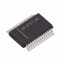
MAX1631EAI+T Maxim Integrated Products, MAX1631EAI+T Datasheet - Page 4

MAX1631EAI+T
Manufacturer Part Number
MAX1631EAI+T
Description
IC PS CTRLR FOR NOTEBOOKS 28SSOP
Manufacturer
Maxim Integrated Products
Type
Step-Down (Buck)r
Datasheet
1.MAX1634CAI.pdf
(29 pages)
Specifications of MAX1631EAI+T
Internal Switch(s)
No
Synchronous Rectifier
Yes
Number Of Outputs
2
Voltage - Output
3.3V, 5V, Adj
Current - Output
4A
Frequency - Switching
200kHz, 300kHz
Voltage - Input
4.2 ~ 30 V
Operating Temperature
-40°C ~ 85°C
Mounting Type
Surface Mount
Package / Case
28-SSOP
Power - Output
762mW
Output Voltage
2.5 V to 5.5 V, 3.3 V, 5 V
Input Voltage
4.2 V to 30 V
Mounting Style
SMD/SMT
Maximum Operating Temperature
+ 85 C
Minimum Operating Temperature
- 40 C
Lead Free Status / RoHS Status
Lead free / RoHS Compliant
Multi-Output, Low-Noise Power-Supply
Controllers for Notebook Computers
ELECTRICAL CHARACTERISTICS (continued)
(V+ = 15V, both PWMs on, SYNC = VL, VL load = 0mA, REF load = 0mA, SKIP = 0V, T
Typical values are at T
4
Note 1: Each of the four digital soft-start levels is tested for functionality; the steps are typically in 20mV increments.
Note 2: High duty-factor operation supports low input-to-output differential voltages, and is achieved at a lowered operating
Note 3: MAX1630/MAX1632/MAX1633/MAX1635 only.
Note 4: Off mode for the 12V linear regulator occurs when the SMPS that has flyback feedback (V
Note 5: Since the reference uses VL as its supply, the reference’s V+ line-regulation error is insignificant.
FAULT DETECTION (MAX1630/MAX1631/MAX1632)
RESET
INPUTS AND OUTPUTS
Overvoltage Trip Threshold
Overvoltage-Fault Propagation Delay
Output Undervoltage Threshold
Output Undervoltage Lockout Time
Thermal Shutdown Threshold
RESET Trip Threshold
RESET Propagation Delay
RESET Delay Time
Feedback Input Leakage Current
Logic Input Low Voltage
Logic Input High Voltage
Input Leakage Current
Logic Output Low Voltage
Logic Output High Current
TIME/ON5 Input Trip Level
TIME/ON5 Source Current
TIME/ON5 On-Resistance
Gate Driver Sink/Source Current
Gate Driver On-Resistance
_______________________________________________________________________________________
frequency (see Overload and Dropout Operation section).
situations where the main outputs are being held up by external keep-alive supplies, turning off the 12OUT regulator pre-
vents a leakage path from the output-referred flyback winding, through the rectifier, and into V
PARAMETER
A
= +25°C.)
With respect to unloaded output voltage
CSL_ driven 2% above overvoltage trip threshold
With respect to unloaded output voltage
From each SMPS enabled, with respect to f
Typical hysteresis = +10°C
With respect to unloaded output voltage,
falling edge; typical hysteresis = 1%
Falling edge, CSL_ driven 2%
below RESET trip threshold
With respect to f
FB3, FB5; SECFB = 2.6V
RUN/ON3, SKIP, TIME/ON5 (SEQ = REF),
SHDN, STEER, SYNC
RUN/ON3, SKIP, TIME/ON5 (SEQ = REF),
SHDN, STEER, SYNC
RUN/ON3, SKIP, TIME/ON5 (SEQ = REF),
SHDN, STEER, SYNC, SEQ; V
RESET, I
RESET = 3.5V
SEQ = 0V or VL
TIME/ON5 = 0V, SEQ = 0V or VL
TIME/ON5; RUN/ON3 = 0V, SEQ = 0V or VL
DL3, DH3, DL5, DH5; forced to 2V
High or low
SINK
= 4mA
OSC
CONDITIONS
PIN
= 0V or 3.3V
OSC
A
= T
MIN
27,000
5000
MIN
DD
2.4
2.4
2.5
60
-7
4
1
to T
) steered to it is disabled. In
DD
MAX
.
32,000
6144
TYP
150
-5.5
, unless otherwise noted.
1.5
1.5
1.5
70
15
7
1
3
1
37,000
MAX
7000
0.6
0.4
2.6
3.5
±1
10
80
50
80
-4
7
UNITS
Clk
Clk
mA
°C
nA
µA
µA
µs
µs
%
%
%
Ω
Ω
V
V
V
V
A


