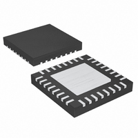
MAX5951ETJ+ Maxim Integrated Products, MAX5951ETJ+ Datasheet - Page 12

MAX5951ETJ+
Manufacturer Part Number
MAX5951ETJ+
Description
IC BUCK PWM CTRLR 12V/5V 32-TQFN
Manufacturer
Maxim Integrated Products
Type
Step-Down (Buck)r
Datasheet
1.MAX5951ETJT.pdf
(25 pages)
Specifications of MAX5951ETJ+
Internal Switch(s)
No
Synchronous Rectifier
No
Number Of Outputs
1
Voltage - Output
0.8 ~ 5.5 V
Current - Output
10A
Frequency - Switching
100kHz ~ 1MHz
Voltage - Input
8 ~ 16 V
Operating Temperature
-40°C ~ 85°C
Mounting Type
Surface Mount
Package / Case
32-TQFN Exposed Pad
Power - Output
2.76W
Lead Free Status / RoHS Status
Lead free / RoHS Compliant
REG is the output terminal of a 5V LDO, which is pow-
ered from IN and provides power to the IC. Bypass
REG to AGND with a 2.2µF ceramic capacitor. Place
the capacitor physically close to the MAX5951 to pro-
vide good bypassing. REG is intended for powering
only the internal circuitry and should not be used to
supply power to external loads.
DREG is the supply input for the low-side MOSFET dri-
ver. Connect DREG to REG externally. Adding an RC
filter (5Ω resistor and 2.2µF ceramic capacitor) from
REG to DREG filters out the high peak currents of the
MOSFET drivers.
BST supplies the power for the high-side MOSFET dri-
vers. Connect the bootstrap diode from BST to DREG
(anode at DREG and cathode at BST). Connect a boot-
strap 1µF ceramic capacitor between BST and LX.
The high-side (DH) and low-side (DL) drivers drive the
gates of the external n-channel MOSFETs. The drivers’
2A peak source-and-sink current capability provides
ample drive to ensure fast rise and fall times of the
switching MOSFETs. Short rise and fall times minimize
switching losses. For low output-voltage applications
where the duty cycle is less than 50%, choose a high-
side MOSFET (Q2) with a moderate R
low-side MOSFET (Q1) with a very low R
The gate driver circuitry also provides a break-before-
make time (25ns, typ) to prevent shoot-through currents
during transition.
Use an external resistor at RT to program the MAX5951
switching frequency from 100kHz to 1MHz.
Choose the appropriate resistor at RT to calculate the
desired output switching frequency (f
Connect an external clock (SYNCOUT from another
MAX5950 or MAX5951) at SYNCIN for external clock
12V/5V Input Buck PWM Controller
12
Oscillator/Synchronization Input (SYNCIN)/
Low-Side MOSFET Driver Supply (DREG)
______________________________________________________________________________________
High-Side MOSFET Driver Supply (BST)
Synchronization Output (SYNCOUT)
f
SW
Internal Linear Regulator (REG)
MOSFET Gate Drivers (DH, DL)
(Hz) = (5 x 10
10
) / R
RT
SW
DS(ON)
(Ω)
):
DS(ON)
. Choose a
.
synchronization. For proper synchronization, the exter-
nal frequency must be at least 20% higher than the
frequency programmed through the RT input. If
SYNCIN is 50% duty cycle, SYNCOUT is shifted by
180°, allowing the reduction of the DC-DC converter
input bypass capacitor.
SYNCOUT is a synchronization signal that is used to
drive the SYNCIN of a second MAX5950 or MAX5951.
The STARTUP input in conjunction with digital soft-start
provides simple ratiometric tracking. When using multi-
ple MAX5950s or MAX5951s, in addition to connecting
SYNCIN and SYNCOUT signals appropriately, connect
the STARTUP of all the devices together. STARTUP syn-
chonizes the soft-start of all the devices’ references, and
hence their respective output voltages track ratiometri-
cally. See Figure 1 and the Typical Operating Circuits.
The STARTUP input has an internal 10µA pullup cur-
rent, but can be driven by external logic. When using
multiple converters, connect the STARTUP of all the
devices together.
The DCENI input must be above V
controller to start. By connecting the DCENI inputs of
multiple devices together and having different start
thresholds (V
trollers can be staggered to provide power sequenc-
ing. Connect a resistive divider from REG to THRESH to
AGND to set the start thresholds of each device.
Connect THRESH to AGND to produce a default
1.220V threshold for DCENI. See Figure 1 and the
Typical Operating Circuits.
The PGOOD outputs and DCENI inputs can be daisy-
chained to generate power sequencing. The PGOOD
output is pulled high when the voltage at SENSE is
above V
from the power-supply output voltage to SENSE to
AGND to set the power-good threshold. See Figure 1
and the Typical Operating Circuits.
Power-Good Sequencing (PGOOD, SENSE)
Startup Sequencing (DCENI, THRESH)
REF
(800mV, typ). Connect a resistive divider
THRESH_
), the startup of the PWM con-
Tracking (STARTUP)
THRESH
for the PWM


