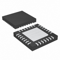
MAX5073ATI+T Maxim Integrated Products, MAX5073ATI+T Datasheet - Page 14

MAX5073ATI+T
Manufacturer Part Number
MAX5073ATI+T
Description
IC CONV BUCK/BOOST 28-TQFN
Manufacturer
Maxim Integrated Products
Type
Step-Down (Buck), Step-Up (Boost)r
Datasheet
1.MAX5073ETI.pdf
(25 pages)
Specifications of MAX5073ATI+T
Internal Switch(s)
Yes
Synchronous Rectifier
No
Number Of Outputs
2
Voltage - Output
0.8 ~ 28 V
Current - Output
1A, 2A
Frequency - Switching
200kHz ~ 2.2MHz
Voltage - Input
4.5 ~ 23 V
Operating Temperature
-40°C ~ 85°C
Mounting Type
Surface Mount
Package / Case
28-TQFN Exposed Pad
Power - Output
2.76W
Lead Free Status / RoHS Status
Lead free / RoHS Compliant
2.2MHz, Dual-Output Buck or Boost Converter
with Internal Power MOSFETs
The MAX5073 dual converter provides separate enable
inputs EN1 and EN2 to individually control or sequence
the output voltages. These active-high enable inputs are
TTL compatible. Pulling EN_ high ramps up the reference
slowly, which provides soft-start at the outputs. Forcing
the EN_ low externally disables the individual output and
generates a PGOOD_ signal. Use EN1, EN2, and
PGOOD1 for sequencing (see Figure 4). Connect
PGOOD1 to EN2 to make sure converter 1’s output is
within regulation before converter 2 starts. Add an RC
network from VL to EN1 and EN2 to delay the individual
converter. A larger RC time constant means a more
delayed output. Sequencing reduces input inrush current
and possible chattering. Connect the EN_ to VL for
always-on operation.
Converter 1 and converter 2 includes a power-good flag,
PGOOD1 and PGOOD2, respectively. Since PGOOD is
an open-drain output and can sink 3mA while providing
the TTL logic-low signal, pull PGOOD to a logic voltage
to provide a logic-level output. PGOOD goes low when
converter 1’s output drops to 92.5% of its nominal regu-
lated voltage. Connect PGOOD to SGND or leave uncon-
nected if not used.
Figure 4. Power-Supply Sequencing Configurations
14
SEQUENCING—OUTPUT 2 DELAYED WITH RESPECT TO OUTPUT 1.
OUTPUT2
______________________________________________________________________________________
VL
VL
DRAIN2
SOURCE2
FB2
EN2
VL
MAX5073
SOURCE1
V+
PGOOD1
DRAIN1
EN1
FB1
VL
PGOOD_
Enable
OUTPUT1
V
IN
R1/C1 AND R2/C2 ARE SIZED FOR REQUIRED SEQUENCING.
The internal switch current of each converter is sensed
using an internal current mirror. Converter 1 and con-
verter 2 have 2A and 1A internal switches. When the
peak switch current crosses the current-limit threshold
of 3A (typ) and 1.8A (typ) for converter 1 and converter
2, respectively, the on cycle is terminated immediately
and the inductor is allowed to discharge. The next
cycle resumes at the next clock pulse.
In deep overload or short-circuit conditions when the
FB voltage drops below 0.4V, the switching frequency
is reduced to 1/4 x f
inductor to discharge. During overload conditions, if the
voltage across the inductor is not high enough to allow
for the inductor current to properly discharge, current
runaway may occur. Current runaway can destroy the
device in spite of internal thermal-overload protection.
Reducing the switching frequency during overload con-
ditions prevents current runaway.
During continuous short circuit or overload at the output,
the power dissipation in the IC can exceed its limit.
Internal thermal shutdown is provided to avoid irreversible
damage to the device. When the die temperature or junc-
tion temperature exceeds +150°C, an on-chip thermal
sensor shuts down the device, forcing the internal switch-
es to turn off, allowing the IC to cool. The thermal sensor
turns the part on again after the junction temperature
cools by +30°C. During thermal shutdown, both regula-
tors shut down, PGOOD_ go low, and soft-start resets.
OUTPUT2
VL
R2
C2
VL
Thermal-Overload Protection
DRAIN2
SOURCE2
FB2
EN2
SW
VL
MAX5073
to provide sufficient time for the
SOURCE1
V+
DRAIN1
EN1
FB1
C1
Current Limit
R1
VL
OUTPUT1
V
IN


