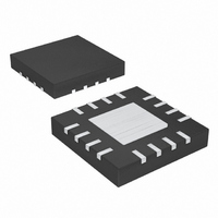
MAX15036ATE+T Maxim Integrated Products, MAX15036ATE+T Datasheet - Page 16

MAX15036ATE+T
Manufacturer Part Number
MAX15036ATE+T
Description
IC DC/DC CONV 3A 16-TQFN-EP
Manufacturer
Maxim Integrated Products
Type
Step-Down (Buck), Step-Up (Boost)r
Datasheet
1.MAX15036ATEVT.pdf
(25 pages)
Specifications of MAX15036ATE+T
Internal Switch(s)
Yes
Synchronous Rectifier
No
Number Of Outputs
1
Voltage - Output
0.6 ~ 28 V
Current - Output
3A
Frequency - Switching
200kHz ~ 2.2MHz
Voltage - Input
4.5 ~ 23 V
Operating Temperature
-40°C ~ 125°C
Mounting Type
Surface Mount
Package / Case
16-TQFN Exposed Pad
Power - Output
2.67W
Lead Free Status / RoHS Status
Lead free / RoHS Compliant
Choose the minimum inductor value so the converter
remains in continuous mode operation at minimum out-
put current (I
where
and I
The V
Schottky diode, D is the duty cycle, and V
age drop across the internal switch. Select the inductor
with low DC resistance and with a saturation current (I
rating higher than the peak switch current limit of 5.6A.
The input current for the boost converter is continuous
and the RMS ripple current at the input is low. Calculate
the capacitor value and ESR of the input capacitor
using the following equations.
where
where V
nal MOSFET plus the voltage drop across the inductor
ESR. ΔI
as calculated above. ΔV
due to the capacitor discharge and ΔV
bution due to ESR of the capacitor.
2.2MHz, 3A Buck or Boost Converters
with an Integrated High-Side Switch
16
______________________________________________________________________________________
OUTMIN
D
P-P
DROP
is the forward voltage drop of the external
L
is the peak-to-peak inductor ripple current
MIN
OUTMIN
= 0.25 x I
is the total voltage drop across the inter-
ΔI
C
=
P P
D
IN
2
−
=
×
=
).
ESR
V
V
f
=
SW
4
OUT
OUT
OUT
(
×
Δ
V
V
Q
I
=
f
IN
P P
×
2
SW
.
IN
is the portion of input ripple
−
+
+
Δ
V
Δ
−
OUT
V
L f
V
V
I
P P
×
×
ESR
V
D
D
×
×
−
DROP
D
Δ
D
−
−
SW
V
×
×
V
V
Q
IN
DS
η
I
OUTMIN
)
×
ESR
Input Capacitor
D
DS
is the contri-
is the volt-
Inductor
SAT
)
For the boost converter, the output capacitor supplies
the load current when the main switch is on. The
required output capacitance is high, especially at high-
er duty cycles. Also, the output capacitor ESR needs to
be low enough to minimize the voltage drop due to the
ESR while supporting the load current. Use the follow-
ing equation to calculate the output capacitor for a
specified output ripple tolerance.
I
due to the capacitor discharge, and ΔV
tribution due to the ESR of the capacitor. D
maximum duty cycle at minimum input voltage.
The MAX15036/MAX15037 are available in thermally
enhanced 16-pin, 5mm x 5mm TQFN packages that
dissipate up to 2.7W at T
perature reaches +170°C, the MAX15036/MAX15037
shut down (see the Thermal-Overload Protection sec-
tion). The power dissipated in the device is the sum of
the power dissipated from supply current (P
dissipated due to switching the internal power MOSFET
(P
rent through the internal power MOSFET (P
The total power dissipated in the package must be lim-
ited so the junction temperature does not exceed its
absolute maximum rating of +150°C at maximum ambi-
ent temperature.
The power dissipated in the switch is:
For the buck converter:
ΔI
OUT
P-P
SW
I
), and the power dissipated due to the RMS cur-
RMS MOSFET
is the load current, ΔV
is the peak-to-peak inductor current ripple.
_
P
MOSFET
C
OUT
=
ESR
= I
(
=
I
OUT
RMS_MOSFET
I
=
OUT
A
Δ
Δ
V
= +70°C. When the die tem-
2
I
Q
OUT
V
Q
×
ESR
×
is the portion of the ripple
D
×
D
)
Power Dissipation
f
MAX
SW
+
⎛
⎜ ⎜
⎝
Δ
Output Capacitor
I
x R
P P
−
12
ESR
ON
2
×
D
is the con-
MAX
Q
MOSFET
⎞
⎟ ⎟
⎠
), power
is the
).


