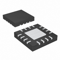
MAX5089ATE+T Maxim Integrated Products, MAX5089ATE+T Datasheet - Page 19

MAX5089ATE+T
Manufacturer Part Number
MAX5089ATE+T
Description
IC DC-DC CONV BUCK 16TQFN
Manufacturer
Maxim Integrated Products
Type
Step-Down (Buck)r
Datasheet
1.MAX5089ATE.pdf
(24 pages)
Specifications of MAX5089ATE+T
Internal Switch(s)
Yes
Synchronous Rectifier
Yes
Number Of Outputs
1
Voltage - Output
0.6 ~ 20 V
Current - Output
2A
Frequency - Switching
200kHz ~ 2.2MHz
Voltage - Input
4.5 ~ 23 V
Operating Temperature
-40°C ~ 125°C
Mounting Type
Surface Mount
Package / Case
16-TQFN Exposed Pad
Power - Output
2.67W
Lead Free Status / RoHS Status
Lead free / RoHS Compliant
When using the MAX5088/MAX5089 in noisy environ-
ments, adjust the controller’s compensation to improve
the system’s noise immunity. In particular, high-fre-
quency noise coupled into the feedback loop causes
duty-cycle jitter. One solution is to lower the crossover
frequency (see the Compensation section).
Careful PC board layout is critical to achieve low-
switching power losses and clean stable operation.
Use a multilayer board whenever possible for better
noise immunity. Follow these guidelines for good PC
board layout:
1) Solder the exposed pad to a large copper plane
2) Isolate the power components and high-current
3) Keep the high-current paths short, especially at the
4) Connect SGND and PGND together close to the
under the IC. To effectively use this copper area as
a heat exchanger between the PC board and the
ambient, expose this copper area on the top and
bottom side of the PC board. Do not make a direct
connection of the exposed pad copper plane to the
SGND (Pin 10) underneath the IC. Connect this
plane and SGND together at the return terminal of
the V+ bypass capacitor
paths from sensitive analog circuitry.
ground terminals. This practice is essential for sta-
ble, jitter-free operation.
return terminals of the V
bypass capacitors near the IC. Do not connect them
together anywhere else.
______________________________________________________________________________________
PC Board Layout Guidelines
Improving Noise Immunity
2.2MHz, 2A Buck Converters with an
L
and V+ high-frequency
Integrated High-Side Switch
5) Keep the power traces and load connections short.
6) Ensure that the feedback connection from FB to
7) Route high-speed switching nodes (BST/VDD,
1) Place the power components (inductor, C
2) Group the gate-drive components (boost diodes
3) Make the ground connections as follows:
This practice is essential for high efficiency. Use
thick copper PC boards to enhance full-load effi-
ciency and power dissipation capability.
C
SOURCE) away from the sensitive analog areas
(BYPASS, COMP, FB, and OSC). Use internal PC
board layers for SGND as EMI shields to keep radi-
ated noise away from the IC, feedback dividers, and
the analog bypass capacitors.
C
other. Make all these connections on the top layer
with wide, copper-filled areas (2oz copper recom-
mended).
and capacitors, and V
near the controller IC.
a) Create a small-signal ground plane underneath
b) Connect this plane to SGND and use this plane
c) Connect SGND and PGND together at the
OUT
OUT
the IC.
for the ground connection for BYPASS, COMP,
FB, and OSC.
return terminal of V+ and V
near the IC. Make this the only connection
between SGND and PGND.
) first, with ground terminals close to each
is short and direct.
L
bypass capacitor) together
Layout Procedure
L
bypass capacitors
IN
, and
19


