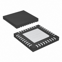
MAX15017BATX+ Maxim Integrated Products, MAX15017BATX+ Datasheet - Page 18

MAX15017BATX+
Manufacturer Part Number
MAX15017BATX+
Description
IC DC/DC CONV 1A 36-TQFN-EP
Manufacturer
Maxim Integrated Products
Type
Step-Down (Buck)r
Datasheet
1.MAX15017AATX.pdf
(26 pages)
Specifications of MAX15017BATX+
Internal Switch(s)
Yes
Synchronous Rectifier
Yes
Number Of Outputs
2
Voltage - Output
1.26 ~ 32 V
Current - Output
1A
Frequency - Switching
135kHz ~ 500kHz
Voltage - Input
7.5 ~ 40 V
Operating Temperature
-40°C ~ 125°C
Mounting Type
Surface Mount
Package / Case
36-TQFN Exposed Pad
Power - Output
2.1W
Lead Free Status / RoHS Status
Lead free / RoHS Compliant
1A, 4.5V to 40V Input Buck Converters with
50mA Auxiliary LDO Regulators
where C
pling capacitance at the buck converter input,
I
cycle, and f
The MAX15014–MAX15017 include UVLO hysteresis
and soft-start to avoid chattering during turn-on.
However, use additional bulk capacitance if the input
source impedance is high. Use enough input capaci-
tance at lower input voltages to avoid possible under-
shoot below the undervoltage lockout threshold during
transient loading.
The allowable output voltage ripple and the maximum
deviation of the output voltage during load steps deter-
mine the output capacitance (C
series resistance (ESR). The output ripple is mainly
composed of ∆V
and ∆V
of the output capacitor). The equations for calculating
the peak-to-peak output voltage ripple are:
Normally, a good approximation of the output voltage rip-
ple is ∆V
tors, assume the contribution to the output voltage ripple
from ESR and the capacitor discharge to be equal to 20%
and 80%, respectively. ∆I
current (see the Input-Capacitor Selection section) and
f
The allowable deviation of the output voltage during
fast load transients also determines the output capaci-
18
OUT_MAX
SW
is the converter’s switching frequency.
______________________________________________________________________________________
ESR
IN
RIPPLE
is the maximum output current, D is the duty
is the sum of C
(caused by the voltage drop across the ESR
SW
D
∆I
P P
=
is the switching frequency.
= ∆V
−
Q
ESR
C
V
∆
∆
OUT
V
IN
(caused by the capacitor discharge)
V
V
=
IN
Q
ESR
ESR
Output-Capacitor Selection
=
(
=
V
=
I
IN
I
OUT MAX
OUT MAX
8
=
+ ∆V
P-P
∆
V
−
×
IN
ESR
V
DRAIN
V
C
Q
_
_
OUT
is the peak-to-peak inductor
×
∆
OUT
Q
×
∆
I
f
SW
P P
×
. If using ceramic capaci-
V
f
SW
−
ESR
OUT
∆
)
and additional decou-
×
×
×
I
+
×
P P
f
D
V
SW
−
L
∆
) and its equivalent
OUT
I
P P
2
−
and
tance, its ESR, and its equivalent series inductance
(ESL). The output capacitor supplies the load current
during a load step until the controller responds with a
greater duty cycle. The response time (t
depends on the closed-loop bandwidth of the converter
(see the Compensation Design section). The resistive
drop across the output capacitor’s ESR, the drop
across the capacitor’s ESL (∆V
discharge causes a voltage droop during the loadstep.
Use a combination of low-ESR tantalum/aluminum elec-
trolytic and ceramic capacitors for better transient load
and voltage ripple performance. Non-leaded capaci-
tors and capacitors in parallel help reduce the ESL.
Keep the maximum output voltage deviation below the
tolerable limits of the electronics being powered. Use
the following equations to calculate the required ESR,
ESL, and capacitance value during a load step:
where I
load step, t
troller and f
The MAX15014–MAX15017 use a voltage-mode control
scheme that regulates the output voltage by comparing
the error amplifier output (COMP) with an internal ramp
to produce the required duty cycle. The output lowpass
LC filter creates a double pole at the resonant frequency,
which has a gain drop of -40dB/decade. The error
amplifier must compensate for this gain drop and
phase shift to achieve a stable closed-loop system.
The basic regulator loop consists of a power modulator,
an output feedback divider, and a voltage error amplifier.
The power modulator has a DC gain set by V
V
output inductance (L), the output capacitance (C
and its ESR. The power modulator incorporates a voltage
feed-forward feature, which automatically adjusts for vari-
ations in the input voltage resulting in a DC gain of 10.
RAMP
, with a double pole and a single zero set by the
STEP
C
RESPONSE
is the load step, t
is the closed-loop crossover frequency.
ESR
C
ESL
t
RESPONSE
OUT
=
=
=
∆
∆
I
STEP
V
V
is the response time of the con-
I
STEP
ESL
ESR
I
STEP
≅
Compensation Design
×
3
×
ƒ
t
1
STEP
STEP
∆
C
t
RESPONSE
V
ESL
Q
is the rise time of the
), and the capacitor
RESPONSE
OUT
IN
),
)
/


