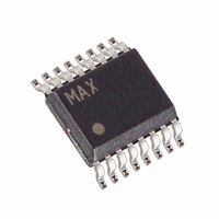
MAX686EEE+ Maxim Integrated Products, MAX686EEE+ Datasheet - Page 14

MAX686EEE+
Manufacturer Part Number
MAX686EEE+
Description
IC SUPPLY LCD BIAS INV 16-QSOP
Manufacturer
Maxim Integrated Products
Type
Step-Up (Boost), Invertingr
Datasheet
1.MAX686EEE.pdf
(16 pages)
Specifications of MAX686EEE+
Internal Switch(s)
Yes
Synchronous Rectifier
No
Number Of Outputs
1
Voltage - Output
±27.5V
Current - Output
100mA
Frequency - Switching
300kHz
Voltage - Input
2.7 ~ 5.5 V
Operating Temperature
-40°C ~ 85°C
Mounting Type
Surface Mount
Package / Case
16-QSOP
Power - Output
667mW
Lead Free Status / RoHS Status
Lead free / RoHS Compliant
R6 turns it off when LCDON goes high. R6 and R7 can
be the same value. Choose R7 such that the minimum
base current is greater than 1/50 of the collector current.
For example, assume V
10mA and then determine R7 as follows:
Remember that the LCD voltage, V
lated output voltage minus the drop across the PNP
switch (300mV typ).
The MAX686 (V
powered from the same source as long as the +5.5V
V
connect V
DAC-Controlled Boost/Inverter
LCD Bias Supply with Internal Switch
14
Figure 8. Using a Common Supply-Voltage Source
V
CC
IN
TO 5.5V
= 2.7V
______________________________________________________________________________________
maximum limit is not violated. To ensure stability,
15 F
R7 ≤ 50 x (12.5 - 0.7) / 10mA = 59k
IN
1 F
and V
CC
R8
100
, V
DD
DD
V
V
DD
CC
directly to the source, connect
) and the inductor (V
OUT(MIN)
MAX686
22 H
Connecting V
DACOUT
LX
FB
= 12.5V and I
OUTSW
MBR0530L
R3
, is the regu-
R1
R2
IN
IN
) can be
to V
LCD
V
OUT
C
CC
F
=
V
bypass V
Figure 8. Since the supply current is very small, the
voltage drop across R8 is insignificant and does not
degrade performance. The RC isolates V
switching noise created by the inductor and internal
power switch.
Although, in many cases, the MAX686 and the inductor
are powered from the same source, it is often advanta-
geous in battery-powered applications to power the
MAX686 IC (V
ply and to power the inductor (V
tery. The MAX686 requires a +2.7V to +5.5V supply at
V
low as 0.8V, significantly increasing usable battery life.
Proper PC board layout is essential due to high current
levels and fast switching waveforms that radiate noise.
It is recommended that initial prototyping be performed
using the MAX686 evaluation kit or equivalent PC
board-based design. Breadboards or proto-boards
should never be used when prototyping switching regu-
lators.
Connect the GND pin, the input bypass-capacitor
ground lead, and the output filter-capacitor ground lead
to a single point (star ground configuration) to minimize
ground noise and improve regulation. Also, minimize
lead lengths to reduce stray capacitance, trace resis-
tance, and radiated noise, with preference given to the
feedback circuit, the ground circuit, and LX. Place R1
and R2 as close to the feedback pin as possible. Place
the bypass capacitors as close to the pins as possible.
Refer to the MAX686 evaluation kit data sheet for an
example of proper board layout.
CC
CC
, but the inductor can be powered from voltages as
to the source through a 100
CC
with a 1µF ceramic capacitor as shown in
CC,
V
DD
) from an available regulated sup-
Layout Considerations
IN
) directly from a bat-
resistor (R8), and
CC
from the


