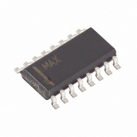
MAX711ESE+ Maxim Integrated Products, MAX711ESE+ Datasheet - Page 9

MAX711ESE+
Manufacturer Part Number
MAX711ESE+
Description
IC DC-DC CONV 16-SOIC
Manufacturer
Maxim Integrated Products
Type
Step-Down (Buck), Step-Up (Boost)r
Datasheet
1.MAX710ESE.pdf
(12 pages)
Specifications of MAX711ESE+
Internal Switch(s)
Yes
Synchronous Rectifier
No
Number Of Outputs
1
Voltage - Output
2.7 ~ 5.5 V
Current - Output
700mA
Voltage - Input
1.8 ~ 11 V
Operating Temperature
-40°C ~ 85°C
Mounting Type
Surface Mount
Package / Case
16-SOIC (3.9mm Width)
Power - Output
696mW
Lead Free Status / RoHS Status
Lead free / RoHS Compliant
Frequency - Switching
-
Lead Free Status / Rohs Status
Lead free / RoHS Compliant
In this configuration, N/E is driven high by LBO when
V
boosts, and the linear regulator operates as a switch,
with minimum forward drop. When V
regulation begins. When V
the linear regulator forces a minimum forward drop of
V
This transition is not seen at the output, since the linear
regulator already has an input-output voltage difference
of 6.5V - 5V. Efficiency with V
V
tion 3 is most suitable when the battery voltage may be
near V
compared with configuration 2, except that two addi-
tional resistors (R5 and R6) are needed.
With N/E connected to PS, when the IC is boosting, the
linear regulator operates with V
cally 0.5V at 5V V
Linear regulation occurs when V
V
cally 10% lower than with the high-efficiency configura-
tions.
The current-limit-select input, ILIM, selects between the
two peak current limits: 1.5A (ILIM = GND) and 0.8A
(ILIM = PS). If the application requires 200mA or less
from the MAX710/MAX711, select 0.8A. The lower peak
current limit permits the use of smaller, low-cost induc-
tors. The ILIM input is internally diode clamped to GND
and PS, and should not be connected to signals out-
side this range.
Grounding SHDN turns off the MAX710/MAX711 com-
pletely, disconnecting the input from the output. Tie
SHDN to PS for normal operation.
The MAX710/MAX711 have a standby mode that shuts
down the step-up converter. The linear regulator
remains on with a 7µA (typ) LDO quiescent current.
Connect STBY to ground to enter standby mode; other-
wise, connect STBY to PS.
For the MAX710, you can obtain a 3.3V or 5V output
voltage by tying 3/5 to GND or PS. Efficiency is typically
85% over a 2mA to 250mA load range. The device is
bootstrapped, with power derived from the step-up
voltage output (at PS). Under all load conditions, the
__________________Design Procedure
FV
OUT
FV
IN
Configuration 3: High Efficiency, 11V, V
(typically 0.5V at 5V V
> 6.5V (Figure 2b). When V
voltage differential results in boost efficiency typi-
is equal to that of configuration 1, so configura-
OUT
. This hookup has no functional shortcomings
Shutdown and Standby Modes
_______________________________________________________________________________________
OUT
Output Voltage Selection
) for optimum noise rejection.
OUT
IN
Configuration 4: Low Noise
> 6.5V (set by R5 and R6),
) as LBO drives N/E high.
FV
IN
IN
forward voltage (typi-
slightly higher than
IN
> V
Step-Up/Down DC-DC Converters
IN
< V
OUT
> V
OUT
BATT
+ V
OUT
, the IC
FV
, linear
< 6.5V
ILIM
. The
MAX710/MAX711 typically start up with a 1V input. If
the battery voltage exceeds the programmed output
voltage, the output will linear regulate down to the
selected output voltage.
The MAX711’s adjustable output voltage is set by two
resistors, R1 and R2 (Figure 3), which form a voltage
divider between the output and FB. Use the following
equation to determine the resistor values:
where V
Since the input bias current at FB has a maximum value
of 50nA, R1 and R2 can be large with no significant
accuracy loss. Choose R2 in the 100kΩ to 1MΩ range
and calculate R1 using the formula above. For 1%
error, the current through R1 should be at least 100
times FB’s bias current.
The MAX710/MAX711 contain a comparator for low-
battery detection. If the voltage at LBI+ falls below that
at LBI- (typically connected to REF), LBO goes low.
Hysteresis is typically 50mV. Set the low-battery moni-
tor’s threshold with two resistors, R3 and R4 (Figure 2),
using the following equation:
Figure 3. MAX711 Adjustable Output Voltage
3.3V/5V or Adjustable,
IN
C1
R4
R3
REF
ON
R1 = R2 [(V
R3 = R4 [(V
= 1.25V.
OFF
SHDN
STBY
N/E
LBO
LBI+
LBI-
REF
OUT
LBT
PGND
Low-Battery Comparator
MAX711
/ V
/ V
LBI
REF
GND
-) - 1]
) - 1]
ILIM
OUT
PS
FB
LX
R1
R2
L1
C4
C2
9


