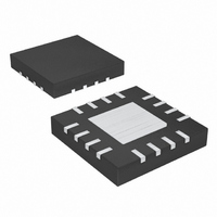
MAX15037ATE+ Maxim Integrated Products, MAX15037ATE+ Datasheet

MAX15037ATE+
Specifications of MAX15037ATE+
Related parts for MAX15037ATE+
MAX15037ATE+ Summary of contents
Page 1
... MOSFET o Power-On-Reset Output (MAX15036)/Power-Good Output (MAX15037) o Short-Circuit Protection (Buck)/Maximum Duty- Cycle Limit (Boost) o Thermal-Shutdown Protection o Thermally Enhanced 16-Pin TQFN Package Dissipates 2.7W PART MAX15036ATE+ MAX15037ATE+ + Denotes a lead-free/RoHS-compliant package Exposed pad. Applications TOP VIEW SYNC RESET FEATURES RESET Output, BST/VDD ...
Page 2
Buck or Boost Converters with an Integrated High-Side Switch ABSOLUTE MAXIMUM RATINGS V+ to PGND............................................................-0.3V to +25V BST/VDD, DRAIN to SGND ....................................-0.3V to +30V SGND to PGND .....................................................-0.3V to +0.3V BST/VDD to SOURCE...............................................-0.3V to +6V SOURCE to SGND..................................................-0.6V ...
Page 3
Buck or Boost Converters with an Integrated High-Side Switch ELECTRICAL CHARACTERISTICS (continued) ( 5.5V to 23V values are +25°C.) (Note ...
Page 4
Buck or Boost Converters with an Integrated High-Side Switch ELECTRICAL CHARACTERISTICS (continued) ( 5.5V to 23V values are +25°C.) (Note ...
Page 5
Buck or Boost Converters with an Integrated High-Side Switch ( 5.2V +25°C, Figures 5 and 6, unless otherwise noted MAX15036 BUCK EFFICIENCY vs. OUTPUT CURRENT (V = 5.5V 2.2MHz) ...
Page 6
Buck or Boost Converters with an Integrated High-Side Switch ( 5.2V +25°C, Figures 5 and 6, unless otherwise noted MAX15037 V DROPOUT VOLTAGE L vs. SWITCHING FREQUENCY 0. 5.5V ...
Page 7
Buck or Boost Converters with an Integrated High-Side Switch ( 5.2V +25°C, Figures 5 and 6, unless otherwise noted MAX15037 SOFT-START AND SHUTDOWN (I = 2A) OUT MAX15036 toc15 V = ...
Page 8
Buck or Boost Converters with an Integrated High-Side Switch PIN NAME Internal Power MOSFET Drain Connection. Buck converter operation—use the MOSFET as a high-side switch 1, 2 DRAIN and connect DRAIN to the input supply. Boost converter operation ...
Page 9
Buck or Boost Converters with an Integrated High-Side Switch V+ DRAIN SYNC CKO OSCILLATOR OSC 2V 1V BYPASS PWM COMPARATOR V REF EN DIGITAL SOFT-START MAX15036 Figure 1. MAX15036 Block Diagram _______________________________________________________________________________________ CURRENT-LIMIT COMPARATOR 4-PULSE SKIP R Q ...
Page 10
Buck or Boost Converters with an Integrated High-Side Switch V+ DRAIN SYNC OSCILLATOR OSC 2V 1V BYPASS PWM COMPARATOR V REF EN DIGITAL SOFT-START MAX15037 Figure 2. MAX15037 Block Diagram 10 ______________________________________________________________________________________ CURRENT-LIMIT COMPARATOR 4-PULSE SKIP R Q ...
Page 11
Buck or Boost Converters with an Integrated High-Side Switch Detailed Description The MAX15036/MAX15037 use a pulse-width modula- tion (PWM) voltage-mode control scheme. The MAX15036 is a nonsynchronous converter and uses an external low-forward-drop Schottky diode for rectifica- tion. ...
Page 12
Buck or Boost Converters with an Integrated High-Side Switch active-high input that turns the MAX15036/ MAX15037 on and off TTL-logic input with 2.0V and 0.8V logic-high and low levels, respectively. When EN ...
Page 13
Buck or Boost Converters with an Integrated High-Side Switch At high input-to-output differential, and high switching frequency, the on-time drops to the order of 100ns. Even though the MAX15036/MAX15037 can control the on-time as low as 100ns, the ...
Page 14
Buck or Boost Converters with an Integrated High-Side Switch Effective Input Voltage Range The MAX15036/MAX15037 can operate with input sup- plies ranging from 4.5V to 5.5V or 5.5V to 23V. The input voltage range (V+) can be constrained ...
Page 15
Buck or Boost Converters with an Integrated High-Side Switch The input ripple comprises mainly of ΔV capacitor discharge) and ΔV (caused by the ESR of ESR the input capacitor). The total voltage ripple is the sum of ΔV ...
Page 16
Buck or Boost Converters with an Integrated High-Side Switch Choose the minimum inductor value so the converter remains in continuous mode operation at minimum out- put current (I ). OUTMIN 2 × × ...
Page 17
Buck or Boost Converters with an Integrated High-Side Switch For the boost converter +(I RMS_MOSFET × V OUT = − ...
Page 18
Buck or Boost Converters with an Integrated High-Side Switch lower than f and close to f ZESR C compensation network where zero (f ) and R C provides a high-frequency pole. ...
Page 19
Buck or Boost Converters with an Integrated High-Side Switch V OUT R1 R2 Figure 3. Type II Compensation Network V OUT Figure 4. Type III Compensation Network ______________________________________________________________________________________ REF ...
Page 20
Buck or Boost Converters with an Integrated High-Side Switch Boost Converter Compensation The boost converter compensation gets complicated due to the presence of a right-half-plane zero f The right-half-plane zero causes a drop in-phase while adding positive (+1) ...
Page 21
Buck or Boost Converters with an Integrated High-Side Switch side of the PCB. Do not make a direct connection of the exposed pad copper plane to the SGND (pin 10) underneath the IC. Connect this plane and SGND ...
Page 22
Buck or Boost Converters with an Integrated High-Side Switch Figure 5. MAX15036 Buck Configuration 22 ______________________________________________________________________________________ ...
Page 23
Buck or Boost Converters with an Integrated High-Side Switch Figure 6. MAX15037 Buck Configuration ______________________________________________________________________________________ 23 ...
Page 24
Buck or Boost Converters with an Integrated High-Side Switch VOUT VOUT C12 C11 0.1μF 22μF PGND VIN VIN C1 C2 47μF 10μF PGND 35V VOUT R3 R1 1kΩ 27.4kΩ 560pF R2 6.04kΩ 1% Figure 7. ...
Page 25
... Maxim cannot assume responsibility for use of any circuitry other than circuitry entirely embodied in a Maxim product. No circuit patent licenses are implied. Maxim reserves the right to change the circuitry and specifications without notice at any time. Maxim Integrated Products, 120 San Gabriel Drive, Sunnyvale, CA 94086 408-737-7600 ____________________ 25 © 2008 Maxim Integrated Products ...


