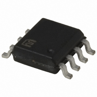
MIC4684BM Micrel Inc, MIC4684BM Datasheet - Page 10

MIC4684BM
Manufacturer Part Number
MIC4684BM
Description
IC REG BUCK 2A ADJ VOLT HE 8SOIC
Manufacturer
Micrel Inc
Series
SuperSwitcher™r
Type
Step-Down (Buck)r
Datasheet
1.MIC4684-3.3BM_TR.pdf
(16 pages)
Specifications of MIC4684BM
Mounting Type
Surface Mount
Internal Switch(s)
Yes
Synchronous Rectifier
No
Number Of Outputs
1
Voltage - Output
Adj to 1.235V
Current - Output
2A
Frequency - Switching
200kHz
Voltage - Input
4 ~ 30 V
Operating Temperature
-40°C ~ 125°C
Package / Case
8-SOIC (3.9mm Width)
No. Of Pins
8
Peak Reflow Compatible (260 C)
No
Current Rating
2A
Output Voltage Max
1.235V
Supply Voltage Max
30V
Leaded Process Compatible
No
Voltage Regulator Type
Switching
Lead Free Status / RoHS Status
Lead free / RoHS Compliant
Power - Output
-
Lead Free Status / RoHS Status
Contains lead / RoHS non-compliant, Lead free / RoHS Compliant
Available stocks
Company
Part Number
Manufacturer
Quantity
Price
Company:
Part Number:
MIC4684BM
Manufacturer:
ST
Quantity:
1 600
Micrel, Inc.
Applications Information
Adjustable Regulators
Adjustable regulators require a 1.23V feedback signal. Rec-
ommended voltage-divider resistor values for common output
voltages are included in Table 1.
For other voltages, the resistor values can be determined
using the following formulas:
Minimum Pulse Width
The minimum duty cycle of the MIC4684 is approximately
10%. See Minimum Duty Cycle Graph. If this input-to-output
voltage characteristic is exceeded, the MIC4684 will skip
cycles to maintain a regulated V
Thermal Considerations
The MIC4684 SuperSwitcher™ features the power-SOP-8.
This package has a standard 8-lead small-outline package
profile, but with much higher power dissipation than a standard
SOP-8. Micrel’s MIC4684 SuperSwitcher™ family are the first
dc-to-dc converters to take full advantage of this package.
The reason that the power SOP-8 has higher power dissipa-
tion (lower thermal resistance) is that pins 2, 6, and 7 and
the die-attach paddle are a single piece of metal. The die is
attached to the paddle with thermally conductive adhesive.
This provides a low thermal resistance path from the junction
of the die to the ground pins. This design significantly improves
package power dissipation by allowing excellent heat transfer
through the ground leads to the printed circuit board.
One limitation of the maximum output current on any MIC4684
design is the junction-to-ambient thermal resistance (θ
the design (package and ground plane).
January 2010
Figure 1. Minimum Pulse Width Characteristic
R1
V
V
OUT
REF
=
R2
=
=
1.235V
V
REF
V
V
OUT
REF
Constant-Frequency Switchin g
40
35
30
25
20
15
10
Max. V
5
0
0
R2
R1
−
1
OUTPUT VOLTAGE (V)
1
+
IN
1
for a Given V
2
3
OUT
4
.
OUT
5
for
6
JA
) of
10
Examining θ
where:
θ
θ
connection of pins 2, 6, and 7 to the ground plane. The pur-
pose of the ground plane is to function as a heat sink.
θ
the ground plane to which the power SOP-8 is attached.
Determining Ground-Plane Heat-Sink Area
Make sure that MIC4684 pins 2, 6, and 7 are connected to
a ground plane with a minimum area of 6cm
plane should be as close to the MIC4684 as possible. The
area may be distributed in any shape around the package
or on any pcb layer as long as there is good thermal contact
to pins 2, 6, and 7. This ground plane area is more than suf-
ficient for most designs.
When designing with the MIC4684, it is a good practice to
connect pins 2, 6, and 7 to the largest ground plane that is
practical for the specific design.
Checking the Maximum Junction Temperature:
For this example, with an output power (P
output at 1A with V
temperature, what is the junction temperature?
Referring to the “Typical Characteristics: 5V Output Efficiency”
graph, read the efficiency (η) for 1A output current at V
12V or perform you own measurement.
The efficiency is used to determine how much of the output
power (P
JC
CA
JA
is ideally 75°C/W, but will vary depending on the size of
is dependent on layout and is primarily governed by the
is a relatively constant 25°C/W for a power SOP-8.
θ
θ
η = 84%
P =
P =
P
θ
JC
CA
D
D
D
JA
OUT
Figure 2. Power SOP-8 Cross Section
= 0.95W
= junction-to-case thermal resistance
= case-to-ambient thermal resistance
= (θ
P
0.84
5W
OUT
JA
) is dissipated in the regulator circuit (P
η
JC
in more detail:
−
+ θ
−
5W
P
IN
OUT
CA
printed circuit board
SOP-8
= 12V) and 60°C maximum ambient
)
θ
JC
θ
JA
θ
CA
heat sink area
ground plane
OUT
2
. This ground
M9999-012610
) of 5W, (5V
MIC4684
D
).
IN
=


