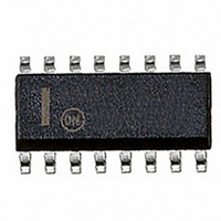
MC34067DW ON Semiconductor, MC34067DW Datasheet - Page 10

MC34067DW
Manufacturer Part Number
MC34067DW
Description
IC CTRLR SMPS DBL END HF 16SOIC
Manufacturer
ON Semiconductor
Type
Flybackr
Datasheet
1.MC34067DWG.pdf
(16 pages)
Specifications of MC34067DW
Internal Switch(s)
No
Synchronous Rectifier
No
Number Of Outputs
1
Current - Output
100mA
Frequency - Switching
525kHz ~ 2.05MHz
Voltage - Input
2.5 ~ 20 V
Operating Temperature
0°C ~ 70°C
Mounting Type
Surface Mount
Package / Case
16-SOIC (0.300", 7.5mm Width)
Power - Output
862mW
Output Voltage Range
5 V to 5.2 V
Input Voltage Range
20 V
Mounting Style
SMD/SMT
Lead Free Status / RoHS Status
Contains lead / RoHS non-compliant
Voltage - Output
-
Lead Free Status / Rohs Status
Lead free / RoHS Compliant
Other names
MC34067DWOS
Available stocks
Company
Part Number
Manufacturer
Quantity
Price
Part Number:
MC34067DW
Manufacturer:
FREESCALE
Quantity:
20 000
power MOSFETs and are capable of sourcing and sinking
1.5 A. Rise and fall times are typically 20 ns and 15 ns
respectfully when driving a 1.0 nF load. High source/sink
capability in a totem−pole driver normally increases the risk
of high cross conduction current during output transitions.
support and protection functions including a precision
voltage reference, undervoltage lockout comparators,
soft−start circuitry, and a fault detector. These peripheral
circuits ensure that the power supply can be turned on and
off in a controlled manner and that the system will be quickly
disabled when a fault condition occurs.
Undervoltage Lockout and Voltage Reference
input V
illustrated in Figure 19. When V
threshold voltage, the V
Reference Regulator. After the V
Regulator rises to 4.2 V, the V
the UVLO signal to a logic zero state enabling the primary
control path. Reducing V
causes the V
Regulator. The V
UVLO output to a logic one state disabling the controller.
designer to select the V
this pin is open, the comparator switches the controller on at
16 V and off at 9.0 V. If this pin is connected to the V
terminal, the upper and lower thresholds are reduced to
9.0 V and 8.6 V, respectively. Forcing the Enable/UVLO
Adjust pin low will pull the V
low (through an internal diode) turning off the controller.
reference to internal circuitry and can deliver up to 10 mA
The totem−pole output drivers are ideally suited for driving
The MC34067 Resonant Controller provides a number of
Separate undervoltage lockout comparators sense the
The Enable/UVLO Adjust pin allows the power supply
The Reference Regulator provides a precise 5.1 V
CC
UVLO Adjust
voltage and the regulated reference voltage as
CC
Enable /
UVLO comparator to disable the Reference
ref
V
CC
UVLO comparator then switches the
15
9
CC
CC
CC
UVLO threshold voltages. When
UVLO comparator enables the
ref
to the lower threshold voltage
CC
7.0k
UVLO comparator switches
ref
CC
UVLO comparator input
output of the Reference
Figure 19. Undervoltage Lockout and Reference
increases to the upper
50k
50k
PERIPHERAL SUPPORT FUNCTIONS
7.0k
8.0 V
http://onsemi.com
CC
V
CC
UVLO
10
The MC34067 utilizes a unique design that virtually
eliminates cross conduction, thus controlling the chip power
dissipation at high frequencies. A separate power ground pin
is provided to isolate the sensitive analog circuitry from large
transient currents.
to external loads. The reference is trimmed to better than 2%
initial accuracy and includes active short circuit protection.
Fault Detection
can be implemented with proper use of the Fault Comparator
and Latch blocks that are illustrated in Figure 20. The Fault
Comparator has an input threshold of 1.0 V and when
exceeded, sets the Fault Latch and generates two logic
signals that simultaneously disable the primary control path.
The signal line labeled “Fault” connects directly to two gates
that control the output drivers. This direct path reduces the
driver turn−off propagation delay to approximately 70 ns.
The Fault Latch output is OR’ed with the UVLO output that
is derived from the V
logic output labeled “UVLO+Fault”. This signal disables
the Oscillator and the One−Shot by forcing both the C
and C
logic “1” that appears at the V
The latch can also be reset after startup by momentarily
pulling the Enable/UVLO Adjust pin low to disable the
Reference. Note that after activation, the Fault Latch will
remain in a set state only as long as V
MC34067. Also, Drive Output B will assume a high state if
the Fault input signal drops below the 1.0 V threshold level
even after the Fault Latch has been set. In some applications
this characteristic could be problematic but it can be easily
remedied by AC coupling Drive Output B.
Converter protection from adverse operating conditions
The Fault Latch is automatically reset during startup by a
Reference
T
5.1 V
capacitors to be continually charged.
UVLO
V
V
ref
ref
ref
UVLO
UVLO comparator, to produce the
4.2/4.0 V
ref
UVLO comparator output.
CC
is provided to the
5
V
ref
OSC


