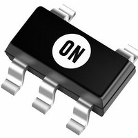
NCP1521ASNT1G ON Semiconductor, NCP1521ASNT1G Datasheet

NCP1521ASNT1G
Specifications of NCP1521ASNT1G
Available stocks
Related parts for NCP1521ASNT1G
NCP1521ASNT1G Summary of contents
Page 1
... CIN GND 2 OFF Figure 1. Typical Application © Semiconductor Components Industries, LLC, 2007 May, 2007 - Rev NCP1521ASNT1G †For information on tape and reel specifications, including part orientation and tape sizes, please refer to our Tape and Reel Packaging Specification Brochure, BRD8011/D. L VOUT COUT R1 Cff R2 1 http://onsemi ...
Page 2
Figure 2. Efficiency vs. Output Current Vbattery VIN PWM/PFM 1 CONTROL 4.7 mF GND 2 LOGIC CONTROL Enable EN & THERMAL 3 SHUTDOWN Figure 3. Simplified Block Diagram NCP1521 V = 3.3 V ...
Page 3
PIN FUNCTION DESCRIPTION Pin No. Symbol Function 1 VIN Analog Input 2 GND Analog/Power Ground 3 EN Digital Input 4 FB Analog Input 5 LX Analog Output MAXIMUM RATINGS Rating Minimum Voltage All Pins Maximum Voltage All Pins (Note 2) ...
Page 4
ELECTRICAL CHARACTERISTICS +85°C ambient temperature, unless otherwise noted, operating conditions V Characteristic Input Voltage Range Undervoltage Lockout (V Falling) IN Quiescent Current PFM No Load Standby Current, EN Low Oscillator Frequency Peak Inductor Current Feedback Reference Voltage FB Pin Tolerance ...
Page 5
V , INPUT VOLTAGE (V) IN Figure 5. Quiescent Current vs. Supply Voltage 1 OUT 0.8 ...
Page 6
EN 2 V/Div V OUT 500 mV/Div 100 ms/Div Figure 11. Soft Start Time (V 1.8 1.7 1.6 1.5 1.4 1 300 mA OUT 1.2 -40 - TEMPERATURE (°C) Figure 13. Frequency vs. Temperature 2.0 ...
Page 7
I = 100 mA OUT 1.0 0 300 mA OUT 0.0 -0 600 mA OUT -1 -2.0 - TEMPERATURE (°C) Figure 17. Output Voltage Accuracy (V ...
Page 8
Overview The NCP1521 uses a constant frequency, current mode step-down architecture. Both the main (P-Channel MOSFET) and synchronous (N-Channel MOSFET) switches are internal. It delivers a constant voltage from either a single Li-Ion or three cell NiMH/NiCd battery to portable ...
Page 9
Cycle-by-Cycle Current Limitation From the block diagram (Figure 3 used to realize cycle-by-cycle current limit protection. The comparator compares the LX pin voltage with the reference voltage, which is biased by a constant current. If the inductor ...
Page 10
Output Voltage Selection The output voltage is programmed through an external resistor divider connected from V OUT For low power consumption and noise immunity, the resistor from FB to GND (R2) should be in the [100 k-600 k] range. If ...
Page 11
Table 3. List of Inductor FDK MIPW3226 Series TDK VLF3010AT Series Taiyo Yuden LQ CBL2012 Coil craft DO1605-T Series Output Capacitor Selection Selecting the proper output capacitor is based on the desired output ripple voltage. Ceramic capacitors with low ESR ...
Page 12
PCB Layout Recommendations Good PCB layout plays an important role in switching mode power conversion. Careful PCB layout can help to minimize ground bounce, EMI noise and unwanted feedback that can affect the performance of the converter. Hints suggested below ...
Page 13
U1 J1 VFVIN VIN GND 4.7 mF Power NCP152x 0 NCP1521 2 CON3 EN ...
Page 14
NCP1521 Figure 29. Board Layout (Top View) Figure 30. Board Layout (Bottom View) http://onsemi.com 14 ...
Page 15
... V X5R 4 SMD Resistor 220 K 5 SMD Inductor 6 I/O Connector can be plugged by BLZ5.08/2 (Weidmüller reference) 7 Jumper Header vertical mount 3*1, 2. Jumper Connector, 400 mils NCP1521 Ref PCB Footprint Manufacturer U1 TSOP-5 On Semiconductor C1 0805 C2 0805 R1, R2, R3 0805 Vishay-Draloric L1 1605 J1 Tyco Electronics/AMP J6 http://onsemi.com 15 ...
Page 16
... C 0.05 H *For additional information on our Pb-Free strategy and soldering details, please download the ON Semiconductor Soldering and Mounting Techniques Reference Manual, SOLDERRM/D. ON Semiconductor and are registered trademarks of Semiconductor Components Industries, LLC (SCILLC). SCILLC reserves the right to make changes without further notice to any products herein. SCILLC makes no warranty, representation or guarantee regarding the suitability of its products for any particular purpose, nor does SCILLC assume any liability arising out of the application or use of any product or circuit, and specifically disclaims any and all liability, including without limitation special, consequential or incidental damages. “ ...


