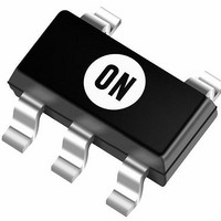
NCP1450ASN30T1G ON Semiconductor, NCP1450ASN30T1G Datasheet

NCP1450ASN30T1G
Specifications of NCP1450ASN30T1G
NCP1450ASN30T1GOS
NCP1450ASN30T1GOSTR
Available stocks
Related parts for NCP1450ASN30T1G
NCP1450ASN30T1G Summary of contents
Page 1
NCP1450A PWM Step−up DC−DC Controller The NCP1450A series are PWM step−up DC−DC switching controller that are specially designed for powering portable equipment from one or two cells battery packs. The NCP1450A series have a driver pin, EXT pin, for connecting ...
Page 2
V IN OUT Reference GND 4 PIN FUNCTION DESCRIPTION Pin # Symbol Á Á Á Á Á 1 Á Á Á Á Á Á CE Á Á Á Á Á Á Á Á Á Á Á Á ...
Page 3
... Device NCP1450ASN19T1 1.9 V NCP1450ASN19T1G NCP1450ASN27T1G 2.7 V NCP1450ASN27T1 NCP1450ASN30T1 3.0 V NCP1450ASN30T1G NCP1450ASN33T1 3.3 V NCP1450ASN33T1G NCP1450ASN50T1 5.0 V NCP1450ASN50T1G †For information on tape and reel specifications, including part orientation and tape sizes, please refer to our Tape and Reel Packaging Specifications Brochure, BRD8011/D. 1. The ordering information lists five standard output voltage device options. Additional devices with output voltage ranging from 1 ...
Page 4
ELECTRICAL CHARACTERISTICS Characteristic OSCILLATOR Frequency ( 0.96, Note 5) OUT SET Frequency Temperature Coefficient (T A Maximum PWM Duty Cycle ( OUT SET Minimum Startup Voltage ( mA) O Minimum Startup Voltage Temperature Coefficient ...
Page 5
1.8 NCP1450ASN19T1 NTGS3446T1 1.7 C OUT T A 1.6 0 200 400 600 I , OUTPUT CURRENT (mA) O Figure 3. ...
Page 6
NCP1450ASN19T1 1 1 1.6 −50 − TEMPERATURE (°C) Figure 9. NCP1450ASN19T1 Output Voltage vs. Temperature 5.2 5.1 5.0 4.9 NCP1450ASN50T1 ...
Page 7
NCP1450ASN19T1 1 0.5 V OUT Open−Loop Test 0 −50 − TEMPERATURE (°C) Figure 15. NCP1450ASN19T1 Standby Current vs. Temperature NCP1450ASN50T1 5.0 ...
Page 8
NCP1450ASN19T1 1 0.96 OUT Open−Loop Test 0 −50 − TEMPERATURE (°C) Figure 21. NCP1450ASN19T1 Oscillator Frequency vs. Temperature 300 250 200 150 100 NCP1450ASN50T1 ...
Page 9
NCP1450ASN19T1 0.96 OUT − − 0.4 V EXT OUT Open−Loop Test −50 −50 − TEMPERATURE (°C) Figure 27. NCP1450ASN19T1 EXT “H” Output Current vs. Temperature ...
Page 10
NCP1450ASN19T1 0.96 5 OUT − 0.4 V EXT OUT Open−Loop Test 0 −50 − TEMPERATURE (°C) Figure 33. NCP1450ASN19T1 EXT “H” ON−Resistance vs. Temperature 25 ...
Page 11
V start 0.6 NCP1450ASN19T1 0 0.4 OUT hold 0.2 0.0 −50 − TEMPERATURE (°C) Figure 39. NCP1450ASN19T1 Startup/Hold Voltage vs. Temperature 1.0 0.8 ...
Page 12
V start 1.6 NCP1450ASN19T1 1 NTGS3446T1 C OUT 0 hold 0.4 0 OUTPUT CURRENT (mA) O Figure 45. NCP1450ASN19T1 Startup/Hold Voltage vs. Output Current ...
Page 13
OUT 220 mF C OUT 1.0 V/div 500 mA/div ...
Page 14
4.7 mH 220 OUT 1.9 V (AC coupled), 200 mV/div OUT 1 100 mA O Figure 57. NCP1450ASN19T1 Load Transient Response = ...
Page 15
V = 1.5 V 2.0 IN 1.9 NCP1450ASN19T1 MMJT9410 1.6 0 200 400 600 I , OUTPUT ...
Page 16
... BJT Semiconductor Á Á Á Á Á Á Á Á Á Á Á Á Á Á Á Á Á Á Á Á Á Á Á Á ...
Page 17
Operation The NCP1450A series are monolithic power switching controllers optimized for battery powered portable products where large output current is required. The NCP1450A series are low noise fixed frequency voltage−mode PWM DC−DC controllers, and consist of startup circuit, feedback resistor ...
Page 18
Step−up Converter Design Equations The NCP1450A PWM step−up DC−DC controller is designed to operate in continuous conduction mode and can be defined by the following equations. External components values can be calculated from these equations, however, the optimized value should ...
Page 19
Diode The diode is the largest source of loss in DC−DC converters. The most importance parameters which affect their efficiency are the forward voltage drop, V reverse recovery time, trr. The forward voltage drop creates a loss just by having ...
Page 20
... Figures 71 and 72. Please contact your Figure 71. NCP1450A PWM Step−up DC−DC Controller Evaluation Board Silkscreen Figure 72. NCP1450A PWM Step−up DC−DC Controller Evaluation Board Artwork (Component Side) NCP1450A ON Semiconductor representative for availability. The evaluation board schematic diagrams are shown in Figures 73 and 74 http://onsemi ...
Page 21
JP1 TP1 OFF TP2 GND Figure 73. NCP1450A Evaluation Board Schematic Diagram 1 (Step−up DC−DC Converter Using External MOSFET Switch) JP2 TP5 OFF TP6 GND Figure ...
Page 22
... H *For additional information on our Pb−Free strategy and soldering details, please download the ON Semiconductor Soldering and Mounting Techniques Reference Manual, SOLDERRM/D. ON Semiconductor and are registered trademarks of Semiconductor Components Industries, LLC (SCILLC). SCILLC reserves the right to make changes without further notice to any products herein ...


