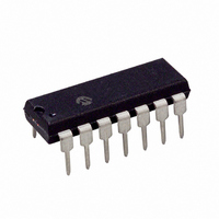
MCP2036-I/P Microchip Technology, MCP2036-I/P Datasheet - Page 4

MCP2036-I/P
Manufacturer Part Number
MCP2036-I/P
Description
IC KEYLESS ENTRY AFE 14-PDIP
Manufacturer
Microchip Technology
Type
Sensor Interfacer
Specifications of MCP2036-I/P
Package / Case
14-DIP (0.300", 7.62mm)
Applications
Analog I/O
Mounting Type
Through Hole
Product
Analog Front End
Supply Voltage (max)
5.5 V
Supply Voltage (min)
2.7 V
Supply Current
6.8 mA
Maximum Operating Temperature
+ 85 C
Minimum Operating Temperature
- 40 C
Mounting Style
Through Hole
Number Of Channels
1
Clock Frequency Max
2MHz
Slew Rate
0.6V/µs
Turn On Time
4µs
Sensor Case Style
DIP
Operating Temperature Range
-40°C To +85°C
No. Of Pins
14
Rohs Compliant
Yes
Supply Voltage Range
2.7 To 5.5V
Lead Free Status / RoHS Status
Lead free / RoHS Compliant
Lead Free Status / RoHS Status
Lead free / RoHS Compliant, Lead free / RoHS Compliant
Available stocks
Company
Part Number
Manufacturer
Quantity
Price
Company:
Part Number:
MCP2036-I/P
Manufacturer:
MICROCHIP
Quantity:
12 000
MCP2036
1.1
The coil driver produces the excitation current for the
sensor coils.
The coil driver input is derived from the digital clock
supplied to the CLK input. The digital signal is first
filtered through a low-pass filter, composed of R
C
create a triangular current in phase and proportional
with the input voltage. Because the digital drive into the
R
DRVIN input will be centered at V
between voltage, current, inductance and frequency is
shown in
EQUATION 1-1:
DS22186C-page 4
IN
IN
ΔV
, and passed to the DRVIN input. The driver will
-C
Note:
ΔI
L
V
F
IN
COIL
OUT
OUT
DRV
DRV
filter has a 50% duty cycle, the voltage on the
Coil Driver
Equation
=
=
=
=
=
(
Pulsed Output Voltage
AC Drive Current Frequency
Inductance of the Sensor Coil
AC Drive Current Amplitude
ΔI
These equations assume a 50% duty cycle.
DRV
1-1.
•
L
COIL
•
2 F
•
DD
DRV
/2. The relationship
)
IN
and
1.2
The Synchronous Detector has two inputs, LREF and
LBTN, selectable by REFSEL. This routes either signal
into the frequency mixer of the detector. The frequency
mixer then converts the AC waveform into a pulsed DC
signal which is amplified and filtered.
The gain of the amplifier is user-settable, using an
external resistor, R
EQUATION 1-2:
An ADC plus firmware algorithm then digitizes the
detector output voltage and uses the resulting data to
detect a key press event.
1.3
To create both an inverting and non-inverting amplifier
topology, a pseudo split supply design is required. To
generate the dual supplies required, a rail splitter is
included, which generates the virtual ground by creat-
ing a voltage output at V
external passive network of the Detector/Amplifier sec-
tion as a reference on the non-inverting input. A bypass
capacitor of 0.1 uF is required to ensure the stability of
the output. For reference accuracy, no more than 3 mA
should be supplied to, or drawn from the reference
output pin.
Note:
Synchronous Detector and Output
Amplifier
Virtual Ground Voltage Reference
Circuit
The
differential connection, so its output is
centered to V
of the detected signal should be calculated
as the difference between voltages at the
output of the detector and the reference
voltage.
Gain R
GAIN
output
∼
(see
DD
© 2009 Microchip Technology Inc.
GAIN
REF
/2. The output is used by the
amplifier/filter
Equation
⁄
(V
10kOhm
DD
/2). The amplitude
1-2).
uses
a


