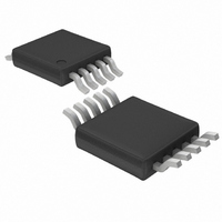
LT3750EMS#PBF Linear Technology, LT3750EMS#PBF Datasheet - Page 9

LT3750EMS#PBF
Manufacturer Part Number
LT3750EMS#PBF
Description
IC CTLR CAPACITOR CHARGE 10-MSOP
Manufacturer
Linear Technology
Type
Flyback, Forward Converterr
Datasheet
1.LT3750EMSPBF.pdf
(16 pages)
Specifications of LT3750EMS#PBF
Applications
Power Supply Controller
Mounting Type
Surface Mount
Package / Case
10-MSOP, Micro10™, 10-uMAX, 10-uSOP
Ic Function
Capacitor Charger Controller
Supply Voltage Range
3V To 24V
Operating Temperature Range
-40°C To +85°C
Digital Ic Case Style
MSOP
No. Of Pins
10
Msl
MSL 1 - Unlimited
Rohs Compliant
Yes
Lead Free Status / RoHS Status
Lead free / RoHS Compliant
Available stocks
Company
Part Number
Manufacturer
Quantity
Price
APPLICATIO S I FOR ATIO
output capacitor is almost completely charged and is
given by:
The output diode’s continuous forward current rating
must exceed I
At a minimum, the diode must satisfy all the previously
mentioned specifications to guarantee proper operation.
However, to optimize charge time, reverse recovery time
and reverse bias leakage current should be considered.
Excessive diode reverse recovery times can cause appre-
ciable discharging of the output capacitor thereby in-
creasing charge time. Choose a diode with a reverse
recovery time of less than 100ns. Diode leakage current
under high reverse bias bleeds the output capacitor of
charge, also increasing charge time. Choose a diode that
has minimal reverse bias leakage current. Table 2 recom-
mends several output diodes for various output voltages
with adequate reverse recovery time.
Table 2. Recommended Output Diodes
MANUFACTURER
Diodes Inc.
(www.diodes.com)
Philips
(www.semiconductors.
philips.com)
Bypass Capacitor Selection
Use a high quality X5R or X7R dielectric ceramic capacitor
placed close to the LT3750 to locally bypass the V
V
capacitor should suffice for V
V
The high peak currents flowing through the transformer
necessitate a larger (>>10µF) capacitor to bypass the pri-
mary winding of the transformer. Inadequate bypassing
TRANS
TRANS
I
AVG D
,
pins. For most applications, a 1µF to 10µF ceramic
pin.
=
2
(
AVG,D
V
OUT PK
I
PK
U
(
.
MURS140
MURS160
NUMBER
BYD147
BYD167
US1M
PART
ES2G
•
)
V
+
TRANS
U
N V
•
CC
TRANS
I
(A)
DC
1
1
2
1
1
1
and a 1µF to 10µF for the
W
REPETITIVE
)
REVERSE
VOLTAGE
PEAK
1000
400
600
400
400
500
(V)
U
PACKAGE
SOD87
SOD87
SMB
SMB
SMB
SMA
CC
and
can result in improper operation. This most often mani-
fests itself in two ways. The first is when the primary wind-
ing current looks distorted instead of triangular. This
substantially reduces the efficiency and increases the
charge time. The second way is when the LT3750 fails to
detect discontinuous mode after the first switching cycle.
Both of these problems are solved by increasing the amount
of capacitive bypassing for the transformer. Choose ca-
pacitors that can handle the high RMS ripple currents
common in flyback regulators.
Output Capacitor Selection
For photoflash applications, the output capacitor will be
discharged into a Xenon flash bulb. Only a pulse capacitor
or photoflash capacitor is able to survive such a harsh
event. Igniting a typical Xenon bulb requires approxi-
mately 250V to 350V stored on a capacitor on the order of
hundreds of microfarads.
Table 3. Recommended Output Capacitor Vendors
VENDOR
Rubycon
Cornell Dubilier
NWL
NMOS Selection
Choose an external NMOS with minimal gate charge and
on resistance that satisfies current limit and voltage break-
down requirements. The gate is nominally driven to V
2V during each charge cycle. Ensure that this does not
exceed the maximum gate to source voltage rating of the
NMOS but enhaces the channel enough to minimize the on
resistance. Similarly, the maximum drain-source voltage
rating of the NMOS must exceed V
magnitude of the leakage inductance spike, whichever is
greater. The maximum instantaneous drain current must
exceed current limit. Because the switching period de-
creases with output voltage, the average current through
the NMOS is greatest when the output is nearly charged
and is given by:
I
AVG M
,
=
2
(
V
OUT PK
I
PK
(
•
)
V
+
OUT PK
N V
(
•
TRANS
WEBSITE
www.rubycon.com
www.cornell-dubilier.com
www.nwl.com
)
TRANS
)
+ V
LT3750
OUT
/N or the
CC
3750fa
9
–


