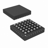
LM8322JGR8X/NOPB National Semiconductor, LM8322JGR8X/NOPB Datasheet - Page 36

LM8322JGR8X/NOPB
Manufacturer Part Number
LM8322JGR8X/NOPB
Description
IC MOBILE I/O COMPAN 36MICRARRAY
Manufacturer
National Semiconductor
Datasheet
1.LM8322JGR8NOPB.pdf
(42 pages)
Specifications of LM8322JGR8X/NOPB
Lead Free Status / RoHS Status
Lead free / RoHS Compliant
Other names
LM8322JGR8X
www.national.com
17.17 READ_CFG COMMAND
The READ_CFG command consists of a command byte
(0x92) from the host and a data byte from the LM8322. The
17.18 WRITE_CLOCK COMMAND
The WRITE_CLOCK command consists of a command byte
(0x93) and a data byte from the host. This command sets the
17.19 READ_CLOCK COMMAND
The READ_CLOCK command consists of a command byte
(0x94) from the host and a data byte from the LM8322. This
7
1
7
1
7
1
MUX2SEL
MUX1SEL
MUX2EN
MUX1EN
Bit
6
0
6
0
6
0
5
0
5
0
5
0
4
1
4
1
4
1
Value
0
1
0
1
0
1
0
1
3
0
3
0
3
0
MUX2_OUT output disabled.
MUX2_OUT output enabled. This overrides any other function available on this pin.
If the MUX2 EN bit is 1, the MUX2_IN1 input drives the MUX2_OUT output.
If the MUX2 EN bit is 1, the MUX2_IN2 input drives the MUX2_OUT output.
MUX1_OUT output disabled.
MUX1_OUT output enabled. This overrides any other function available on this pin.
If the MUX1 EN bit is 1, the MUX1_IN1 input drives the MUX1_OUT output.
If the MUX1 EN bit is 1, the MUX1_IN2 input drives the MUX1_OUT output.
2
0
2
0
2
1
1
1
1
1
1
0
0
1
0
0
0
0
36
7
7
0
7
data byte returns the settings in the hardware configuration
register. The default state of this register is 0x80.
clock configuration, as described in Table 2, Section 9.3
CLOCK CONFIGURATION.
command reads bits 7:2 of the clock configuration, as de-
scribed in Table 2 , Section 9.3 CLOCK CONFIGURATION.
6
6
6
0
Description
CONFIGURATION
5
5
5
0
CONFIGURATION
4
4
0
4
3
3
3
2
2
2
1
1
1
1
0
0
0
0


