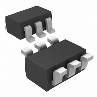
MAX4838EXT+T Maxim Integrated Products, MAX4838EXT+T Datasheet - Page 6

MAX4838EXT+T
Manufacturer Part Number
MAX4838EXT+T
Description
IC CTLR OVP 7.4V SC70-6
Manufacturer
Maxim Integrated Products
Type
Overvoltage protectionr
Datasheet
1.MAX4840EXTT.pdf
(11 pages)
Specifications of MAX4838EXT+T
Applications
Cell Phones, Digital Cameras, Media Players
Mounting Type
Surface Mount
Package / Case
SC-70-6, SC-88, SOT-363
Lead Free Status / RoHS Status
Lead free / RoHS Compliant
Overvoltage-Protection Controllers with
Status FLAG
Figure 5. Functional Diagram
The MAX4838A/MAX4840A/MAX4842A provide up to
+28V overvoltage protection for low-voltage systems.
When the input voltage exceeds the overvoltage trip level,
the MAX4838A/MAX4840A/MAX4842A turn off a low-cost
external n-channel FET(s) to prevent damage to the pro-
tected components. An internal charge pump (Figure 5)
drives the FET gate for a simple, robust solution.
The MAX4838A/MAX4840A have a fixed 3.25V typical
undervoltage-lockout level (UVLO) while the MAX4842A
has a 2.5V typical UVLO. When V
UVLO, the GATE driver is held low and FLAG is asserted.
The MAX4838A has a 7.4V typical overvoltage threshold
(OVLO), and the MAX4840A has a 5.8V typical overvolt-
age threshold. The MAX4842A has a 4.7V typical over-
voltage threshold. When V
GATE driver is held low and FLAG is asserted.
The FLAG output is used to signal the host system
there is a fault with the input voltage. FLAG asserts
immediately to an overvoltage fault. FLAG is held low
for 50ms after GATE turns on before deasserting.
All devices have an open-drain FLAG output. Connect
a pullup resistor from FLAG to the logic I/O voltage of
the host system.
EN is an active-low enable input. Drive EN low or con-
nect to ground to enable normal device operation.
Drive EN high to force the external MOSFET(s) off. EN
does not override an OVLO or UVLO fault.
6
_______________________________________________________________________________________
Undervoltage Lockout (UVLO)
Overvoltage Lockout (OVLO)
Detailed Description
IN
GND
EN
IN
is greater than OVLO, the
EN Enable Input
IN
FLAG Output
is less than the
REGULATOR
UVLO AND
DETECTOR
OVLO
5.5V
LOGIC AND TIMER
2x CHARGE
CONTROL
An on-chip charge pump is used to drive GATE above
IN, allowing the use of low-cost n-channel MOSFETS.
The charge pump operates from the internal 5.5V
regulator.
The actual GATE output voltage tracks approximately
two times V
level is exceeded, whichever comes first. The
MAX4838A has a 7.4V typical OVLO; therefore GATE
remains relatively constant at approximately 10.5V for
5.5V < V
OVLO, but this can be as low as 5.5V. The MAX4840A
in practice may never actually achieve the full 10.5V
GATE output. The MAX4842A has a 4.7V (typ) OVLO,
and the GATE output voltage is 2x the input voltage.
The GATE output voltage as a function of input voltage
is shown in the Typical Operating Characteristics.
The MAX4838A/MAX4840A/MAX4842A have an on-
board state machine to control device operation. A
flowchart is shown in Figure 6. On initial power-up, if
V
FLAG is low.
If UVLO < V
startup after a 50ms internal delay. The internal charge
pump is enabled, and GATE begins to be driven above
V
ing startup until the FLAG blanking period expires, typi-
cally 50ms after the GATE starts going high. At this
point the device is in its on state.
At any time if V
low and GATE is driven to ground.
PUMP
IN
IN
< UVLO or if V
by the internal charge pump. FLAG is held low dur-
IN
IN
< 7.4V. The MAX4840A has a 5.8V typical
IN
GATE DRIVER
MAX4838A
MAX4840A
MAX4842A
< OVLO and EN is low, the device enters
until V
IN
IN
drops below UVLO, FLAG is driven
IN
> OVLO, GATE is held at 0V, and
exceeds 5.5V or the OVLO trip
GATE
FLAG
Device Operation
GATE Driver


