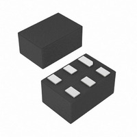
MAX4926ELT+T Maxim Integrated Products, MAX4926ELT+T Datasheet - Page 5

MAX4926ELT+T
Manufacturer Part Number
MAX4926ELT+T
Description
IC CTLR OVP W/EXT PFET 6-UDFN
Manufacturer
Maxim Integrated Products
Datasheet
1.MAX4925ELTT.pdf
(7 pages)
Specifications of MAX4926ELT+T
Applications
*
Mounting Type
Surface Mount
Package / Case
6-µDFN
Lead Free Status / RoHS Status
Lead free / RoHS Compliant
The MAX4923–MAX4926 overvoltage protection
controllers protect low-voltage systems against high-
voltage faults of up to +28V when used with a -30V
pFET. When the input voltage exceeds the OVLO
threshold, these devices turn off the external pFET to
prevent damage to protected components.
The typical overvoltage trip level is set to 7.18V
(MAX4923), 6.16V (MAX4924), 5.65V (MAX4925), and
4.46V (MAX4926). When the supply drops below the
UVLO threshold, the devices turn off the external pFET.
IN is ESD protected to +15kV (Human Body Model) when
bypassed with a 1µF ceramic capacitor to ground.
The MAX4923–MAX4926 have a fixed 2.44V (typ)
UVLO level. When V
and FLAG is high.
The MAX4923 has a 7.18V (typ) OVLO; the MAX4924
has a 6.16V (typ) OVLO; the MAX4925 has a 5.65V
(typ) OVLO; and the MAX4926 has a 4.46V (typ) OVLO.
When V
FLAG is high.
The open-drain FLAG output is used to signal to the
host system that there is a fault with the input voltage.
FLAG goes high during an overvoltage or undervoltage
fault. Connect a pullup resistor from FLAG to the logic
I/O voltage of the host system.
Figure 2. State Machine
V
IN
< V
UVLO
IN
is greater than V
Undervoltage Lockout (UVLO)
_______________________________________________________________________________________
Overvoltage Lockout (OVLO)
IN
Detailed Description
V
is less than V
UVLO
TIME STARTS
GATE = HIGH
FLAG = HIGH
GATE = LOW
FLAG = LOW
COUNTING
STANDBY
< V
ON
IN
t = 20ms
OVLO
< V
OVLO
, GATE is high and
UVLO
FLAG Output
, GATE is high
V
IN
> V
Overvoltage Protectors with
OVLO
The MAX4923–MAX4926 have an on-board state
machine to control device operation. A flowchart is
shown in Figure 2. At initial power up, if V
if V
V
and the device enters its on state after a 20ms delay. At
any time if V
both GATE and FLAG transition high.
In a typical application for the MAX4926, an external
adapter with built-in battery charger is connected to IN
and a battery is connected to the drain of the external
FET. When the adapter is unplugged, IN is directly con-
nected to the battery through the external FET. Since
the battery voltage is typically greater than V
GATE voltage stays low and the device remains pow-
ered by the battery.
The MAX4923–MAX4926 are designed for use with
either a single pFET or dual pFETs in parallel.
MOSFETs with R
recommended. For input supplies near the UVLO maxi-
mum of 2.5V, use a MOSFET specified for a lower V
voltage. Also, the V
must be higher than the V
to withstand the full +28V input range of the
MAX4923–MAX4926.
Figure 3. MAX4926 Typical Operating Circuit
UVLO
ADAPTER WITH
IN
CHARGER
BATTERY
BUILT-IN
> V
< V
OVLO
IN
IN
< V
1
, both GATE and FLAG are high. When
INPUT
2
drops below V
DS(ON)
OVLO
IN
Application Information
GND
DS
MAX4926
External pFET
, an internal timer starts counting
must be -30V and the V
specified for a V
GATE
FLAG
OVLO
MAX4926 Application
4
3
V
UVLO
MOSFET Selection
I0
(max) for the MOSFET
P
Device Operation
LITHIUM ION
BATTERY
OUTPUT
or above V
GS
IN
of -4.5V are
< V
+
-
UVLO
GS
UVLO
SYSTEM
LOADS
OVLO
(max)
, the
GS
or
5
,


