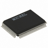
KS8995MA Micrel Inc, KS8995MA Datasheet - Page 35

KS8995MA
Manufacturer Part Number
KS8995MA
Description
IC SWITCH 10/100 5PORT 128PQFP
Manufacturer
Micrel Inc
Specifications of KS8995MA
Applications
*
Mounting Type
Surface Mount
Package / Case
128-MQFP, 128-PQFP
Number Of Primary Switch Ports
5
Internal Memory Buffer Size
64
Operating Supply Voltage (typ)
1.8/2.5/3.3V
Fiber Support
Yes
Integrated Led Drivers
Yes
Phy/transceiver Interface
MII/SNI
Power Supply Type
Analog/Digital
Package Type
PQFP
Data Rate (typ)
10/100Mbps
Vlan Support
Yes
Operating Temperature (max)
70C
Operating Temperature (min)
0C
Pin Count
128
Mounting
Surface Mount
Jtag Support
No
Operating Temperature Classification
Commercial
Data Rate
100Mbps
Lead Free Status / RoHS Status
Lead free / RoHS Compliant
For Use With
576-1017 - BOARD EVAL EXPERIMENT KS8995M
Lead Free Status / RoHS Status
Not Compliant, Lead free / RoHS Compliant
Available stocks
Company
Part Number
Manufacturer
Quantity
Price
Company:
Part Number:
KS8995MAI
Manufacturer:
MAXIM
Quantity:
4 430
I
If a 2-wire EEPROM exists, the KS8995MA can perform more advanced features like broadcast storm protection and rate
control. The EEPROM should have the entire valid configuration data from Register 0 to Register 109 defined in the “Memory
Map,” except the status registers. After reset, the KS8995MA will start to read all 110 registers sequentially from the EEPROM.
The configuration access time (t
To configure the KS8995MA with a pre-configured EEPROM use the following steps:
Note: For proper operation, make sure that pin 47 (PWRDN_N) is not asserted during the reset operation.
SPI Slave Serial Bus Configuration
The KS8995MA can also act as an SPI slave device. Through the SPI, the entire feature set can be enabled, including “VLAN,”
“IGMP snooping,” “MIB counters,” etc. The external master device can access any register from Register 0 to Register 127
randomly. The system should configure all the desired settings before enabling the switch in the KS8995MA. To enable the
switch, write a "1" to Register 1 bit 0.
Two standard SPI commands are supported (00000011 for “READ DATA,” and 00000010 for “WRITE DATA”). To speed
configuration time, the KS8995MA also supports multiple reads or writes. After a byte is written to or read from the KS8995MA,
the internal address counter automatically increments if the SPI Slave Select Signal (SPIS_N) continues to be driven low. If
SPIS_N is kept low after the first byte is read, the next byte at the next address will be shifted out on SPIQ. If SPIS_N is kept
low after the first byte is written, bits on the Master Out Slave Input (SPID) line will be written to the next address. Asserting
SPIS_N high terminates a read or write operation. This means that the SPIS_N signal must be asserted high and then low again
before issuing another command and address. The address counter wraps back to zero once it reaches the highest address.
Therefore the entire register set can be written to or read from by issuing a single command and address.
The KS8995MA is able to support a 5MHz SPI bus. A high performance SPI master is recommended to prevent internal counter
overflow.
May 2005
KS8995MA
2
C Master Serial Bus Configuration
1. At the board level, connect pin 110 on the KS8995MA to the SCL pin on the EEPROM. Connect pin 111 on the
2. Set the input signals PS[1:0] (pins 113 and 114, respectively) to “00.” This puts the KS8995MA serial bus
3. Be sure the board-level reset signal is connected to the KS8995MA reset signal on pin 115 (RST_N).
4. Program the contents of the EEPROM before placing it on the board with the desired configuration data. Note that
5. Place EEPROM on the board and power up the board. Assert the active-low board level reset to RST_N on the
KS8995MA to the SDA pin on the EEPROM.
configuration into I
the first byte in the EEPROM must be “95” for the loading to occur properly. If this value is not correct, all other data
will be ignored.
KS8995MA. After the reset is de-asserted, the KS8995MA will begin reading configuration data from the EEPROM.
The configuration access time (t
RST_N
SCL
SDA
2
C master mode.
prgm
) is less than 15ms as shown in Figure 7.
prgm
) is less than 15ms.
Figure 7. KS8995MA EEPROM
Configuration Timing Diagram
35
t
prgm
....
....
....
<15 ms
M9999-051305
Micrel, Inc.


