VO2631 Vishay, VO2631 Datasheet - Page 4
VO2631
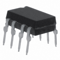
Manufacturer Part Number
VO2631
Description
OPTOCPLR 10MBD 2CH 5KV/US 8DIP
Manufacturer
Vishay
Specifications of VO2631
Voltage - Isolation
5300Vrms
Number Of Channels
2, Unidirectional
Current - Output / Channel
50mA
Data Rate
10MBd
Propagation Delay High - Low @ If
50ns @ 7.5mA
Current - Dc Forward (if)
15mA
Input Type
DC
Output Type
Open Collector
Mounting Type
Through Hole
Package / Case
8-DIP (0.300", 7.62mm)
Maximum Fall Time
0.007 us
Minimum Forward Diode Voltage
1.1 V
Output Device
Logic Gate Photo IC
Configuration
2 Channel
Maximum Baud Rate
10 MBps
Maximum Forward Diode Voltage
1.7 V
Maximum Reverse Diode Voltage
5 V
Maximum Power Dissipation
60 mW
Maximum Operating Temperature
+ 100 C
Minimum Operating Temperature
- 40 C
No. Of Channels
2
Optocoupler Output Type
Logic Gate
Input Current
10mA
Output Voltage
7V
Opto Case Style
DIP
No. Of Pins
8
Propagation Delay Low-high
49ns
Isolation Voltage
5.3kV
Rohs Compliant
Yes
Lead Free Status / RoHS Status
Lead free / RoHS Compliant
Lead Free Status / RoHS Status
Lead free / RoHS Compliant, Lead free / RoHS Compliant
Other names
751-1381-5
VO2631
VO2631
Available stocks
Company
Part Number
Manufacturer
Quantity
Price


Notes
(1)
(2)
Document Number: 84732
Rev. 1.3, 06-Oct-08
SWITCHING CHARACTERISTICS
PARAMETER
Propagation delay time to high
output level
Propagation delay time to low
output level
Pulse width disortion
Propagation delay skew
Output rise time (10 to 90 %)
Output fall time (90 to 10 %)
Propagation delay time of
enable from V
Propagation delay time of
enable from V
Over recommended temperature (T
All typicals at T
75 ns applies to the 6N137 only, a JEDEC registered specification
Pulse gen.
Z = 50 Ω
t = t = 5 ns
f
o
Inpu t I
monitoring
node
r
F
EH
EL
R
amb
to V
to V
M
The probe and Jig capacitances are included in C
= 25 °C, V
EH
EL
I
F
1
2
3
4
Pulse gen.
Z = 50 Ω
t = t = 5 n s
Single channel
f
CC
o
6N137, VO2601, VO2611, VO2630, VO2631, VO4661
Input
monitoring
node
18963-5
= 5 V.
r
For technical questions, contact: optocoupler.answers@vishay.com
amb
V
GND
R
R
R
R
R
R
R
R
V
OUT
L
V
L
V
L
L
L
L
L
L
CC
V
R M
= - 40 °C to + 100 °C), V
TEST CONDITION
Fig. 1 - Single Channel Test Circuit for t
= 350 Ω, C
EL
= 350 Ω, C
EL
E
= 350 Ω, C
= 350 Ω, C
= 350 Ω, C
= 350 Ω, C
= 350 Ω, C
= 350 Ω, C
Fig. 2 - Dual Channel Test Circuit for t
I F
High Speed Optocoupler, 10 MBd
= 0 V, V
= 0 V, V
8
6
5
7
V
CC
1
0.1 µF
bypass
2
3
4
(1)
Dual channel
L
EH
L
EH
L
L
L
L
L
L
= 15 pF,
= 15 pF,
= 15 pF
= 15 pF
= 15 pF
= 15 pF
= 15 pF
= 15 pF
= 3 V
= 3 V
R
C = 15 pF
L
L
Output V
monitoring
node
GND
V CC
CC
L
6
5
8
7
= 5 V, I
O
|t
bypass
SYMBOL
0.1 µF
PHL
Output V
Input I
F
t
t
t
t
t
t
t
PLH
PLH
PHL
PHL
PSK
ELH
EHL
= 7.5 mA unless otherwise specified.
t
t
- t
r
f
PLH
PLH
PLH
F
V CC
O
R L
, t
|
C L = 1 5 p F
, t
PHL
PHL
t
PHL
, t
, t
Output V
monitoring
node
r
r
and t
and t
MIN.
20
25
f
O
f
Vishay Semiconductors
TYP.
2.9
48
50
23
12
11
8
7
t
18964-2
PLH
1.5 V
V
I
I
OL
0 mA
F
F
= 7.5 mA
= 3.75 mA
V
MAX.
75
75
100
100
OH
35
40
(2)
(2)
www.vishay.com
UNIT
ns
ns
ns
ns
ns
ns
ns
ns
ns
ns
177
Related parts for VO2631
Image
Part Number
Description
Manufacturer
Datasheet
Request
R

Part Number:
Description:
357-036-542-201 CARDEDGE 36POS DL .156 BLK LOPRO
Manufacturer:
Vishay
Datasheet:
Part Number:
Description:
357-036-542-201 CARDEDGE 36POS DL .156 BLK LOPRO
Manufacturer:
Vishay
Datasheet:
Part Number:
Description:
357-036-542-201 CARDEDGE 36POS DL .156 BLK LOPRO
Manufacturer:
Vishay
Datasheet:
Part Number:
Description:
357-036-542-201 CARDEDGE 36POS DL .156 BLK LOPRO
Manufacturer:
Vishay
Datasheet:
Part Number:
Description:
357-036-542-201 CARDEDGE 36POS DL .156 BLK LOPRO
Manufacturer:
Vishay
Datasheet:
Part Number:
Description:
357-036-542-201 CARDEDGE 36POS DL .156 BLK LOPRO
Manufacturer:
Vishay
Datasheet:
Part Number:
Description:
357-036-542-201 CARDEDGE 36POS DL .156 BLK LOPRO
Manufacturer:
Vishay
Datasheet:
Part Number:
Description:
357-036-542-201 CARDEDGE 36POS DL .156 BLK LOPRO
Manufacturer:
Vishay
Datasheet:
Part Number:
Description:
357-036-542-201 CARDEDGE 36POS DL .156 BLK LOPRO
Manufacturer:
Vishay
Datasheet:
Part Number:
Description:
357-036-542-201 CARDEDGE 36POS DL .156 BLK LOPRO
Manufacturer:
Vishay
Datasheet:
Part Number:
Description:
357-036-542-201 CARDEDGE 36POS DL .156 BLK LOPRO
Manufacturer:
Vishay
Datasheet:
Part Number:
Description:
357-036-542-201 CARDEDGE 36POS DL .156 BLK LOPRO
Manufacturer:
Vishay
Datasheet:
Part Number:
Description:
357-036-542-201 CARDEDGE 36POS DL .156 BLK LOPRO
Manufacturer:
Vishay
Datasheet:
Part Number:
Description:
357-036-542-201 CARDEDGE 36POS DL .156 BLK LOPRO
Manufacturer:
Vishay
Datasheet:
Part Number:
Description:
357-036-542-201 CARDEDGE 36POS DL .156 BLK LOPRO
Manufacturer:
Vishay
Datasheet: