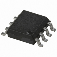
HCPL-0302-060 Avago Technologies US Inc., HCPL-0302-060 Datasheet

HCPL-0302-060
Specifications of HCPL-0302-060
Related parts for HCPL-0302-060
HCPL-0302-060 Summary of contents
Page 1
... The voltage and current supplied by this optocoupler makes it ideally suited for directly driv- ing small or medium power IGBTs. For IGBTs with higher ratings, the HCPL-0314/3140 (0.6 A), HCPL-3150 (0 HCPL-3120 (2.5 A) gate drive opto-couplers can be used. Functional Diagram N/C 1 ANODE ...
Page 2
... XXXE = Lead Free Option HCPL-0302-XXXX No option = Standard SO-8 package, 100 per tube 500 = Tape and Reel Packaging Option 060 = IEC/EN/DIN EN 60747-5-2, V XXXE = Lead Free Option Package Outline Drawings HCPL-3020 Standard DIP Package 9.65 ± 0.25 (0.380 ± 0.010 TYPE NUMBER A XXXXZ ...
Page 3
... HCPL-3020 Gull Wing Surface Mount Option 300 9.65 ± 0.25 (0.380 ± 0.010 1.19 (0.047) MAX. 1.080 ± 0.320 (0.043 ± 0.013) 2.54 (0.100) BSC DIMENSIONS IN MILLIMETERS (INCHES). LEAD COPLANARITY = 0.10 mm (0.004 INCHES). HCPL-0302 Small Outline SO-8 Package XXX 3.937 ± 0.127 YWW (0.155 ± ...
Page 4
Solder Reflow Temperature Profile 300 PREHEATING RATE 3˚C + 1˚C/–0.5˚C/SEC. REFLOW HEATING RATE 2.5˚C ± 0.5˚C/SEC. 200 160˚C 150˚C 140˚C 3˚C + 1˚C/–0.5˚C 100 PREHEATING TIME 150˚ SEC ROOM TEMPERATURE Note: Use of non-chlorine-activated ...
Page 5
... Approved under: IEC 60747-5-2:1997 + A1:2002 EN 60747-5-2:2001 + A1:2002 DIN EN 60747-5-2 (VDE 0884 Teil 2):2003-01. (Option 060 only) IEC/EN/DIN EN 60747-5-2 Insulation Characteristics (HCPL-3020 and HCPL-0302 Option 060) Description Installation Classification per DIN VDE 0110/1.89, Table 1 for Rated Mains Voltage 150 V rms for Rated Mains Voltage 300 V ...
Page 6
... Insulation and Safety Related Specifications Parameter Symbol HCPL-3020 HCPL-0302 Units Conditions Minimum External Air Gap L(101) (Clearance) Minimum External Tracking L(102) (Creepage) Minimum Internal Plastic Gap (Internal Clearance) Tracking Resistance CTI (Comparative Tracking Index) Isolation Group Absolute Maximum Ratings Parameter Storage Temperature ...
Page 7
Electrical Specifications (DC) Over recommended operating conditions unless otherwise specified. Parameter Note High Level Output Current Low Level Output Current High Level Output Voltage Low Level Output Voltage High Level Supply Current Low Level Supply Current Threshold Input Current Low ...
Page 8
Package Characteristics Parameter Symbol Input-Output Momentary Withstand Voltage Input-Output Resistance Input-Output Capacitance Notes: 1. Derate linearly above 70°C free air temperature at a rate of 0.3 mA/°C. 2. Maximum pulse width = 10 µs, maximum duty cycle = 0.2%. This ...
Page 9
I – OUTPUT LOW CURRENT – Figure 3.5 3.0 2.5 2.0 1.5 -50 - 100 125 ...
Page 10
I – FORWARD LED CURRENT – Figure 13. Transfer characteristics 500 Ω + – ...
Page 11
... IGBT drain from turning on the HCPL-3020 or HCPL-0302 270 Ω 2 CONTROL 3 INPUT 74XXX 4 OPEN COLLECTOR Figure 17. Recommended LED drive and application circuit for HCPL-3020 and HCPL-0302. 11 specification of OL HCPL-3020/0302 8 0.1 µF + – ...
Page 12
... Selecting the Gate Resistor (R ) for HCPL-3020 g Step 1: Calculate R minimum from the I g simple RC circuit with a voltage supplied by the HCPL-3020. R ≤ V – OLPEAK = 0.4 = 57.5 Ω The V value the previous equation is the V OL Step 2: Check the HCPL-3020 power dissipation and increase equal to the sum of the emitter power (P ...
Page 13
... Without a detector shield, the dominant cause of optocou- pler CMR failure is capacitive coupling from the input side of the optocoupler, through the package, to the detector IC as shown in Figure 19. The HCPL-3020 and HCPL-0302 improve CMR performance by using a detector IC with an optically transparent Faraday shield, which diverts the capacitively coupled current away from the sensitive IC circuitry ...
Page 14
... Figure 25. The maximum dead time for the HCPL-3020 and HCPL-0302 0.5 µs – (–0.5 µs)) over the operating temperature range of –40°C to 100°C. Note that the propagation delays used to calculate PDD and dead time are ...
Page 15
I LED1 V OUT1 OFF V OUT2 I LED2 t PHL MAX t PLH MIN PDD* MAX = ( PHL PLH *PDD = PROPAGATION DELAY DIFFERENCE NOTE: FOR PDD CALCULATIONS THE PROPAGATION DELAYS ARE TAKEN ...


