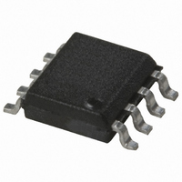
HCPL-0314-500E Avago Technologies US Inc., HCPL-0314-500E Datasheet

HCPL-0314-500E
Specifications of HCPL-0314-500E
Available stocks
Related parts for HCPL-0314-500E
HCPL-0314-500E Summary of contents
Page 1
... The voltage and current supplied by this optocoupler makes it ideally suited for directly driving small or medium power IGBTs. For IGBTs with higher ratings, the HCPL-3150 (0 HCPL-3120 (2.0 A) opto-couplers can be used. Functional Diagram N/C ...
Page 2
... HCPL-0314 -000E No option -500E #500 HCPL-0314 -060E #060 -560E #560 Package Outline Drawings HCPL-3140 Standard DIP Package 9.65 ± 0.25 (0.380 ± 0.010 TYPE NUMBER A XXXXZ YYWW 1.19 (0.047) MAX. 3.56 ± 0.13 (0.140 ± 0.005) 1.080 ± 0.320 (0.043 ± ...
Page 3
... HCPL-3140 Gull Wing Surface Mount Option 300 Outline Drawing 9.65 ± 0.25 (0.380 ± 0.010 1.19 (0.047) MAX. 1.080 ± 0.320 (0.043 ± 0.013) 2.54 (0.100) BSC DIMENSIONS IN MILLIMETERS (INCHES). LEAD COPLANARITY = 0.10 mm (0.004 INCHES). NOTE: FLOATING LEAD PROTRUSION IS 0.25 mm (10 mils) MAX. ...
Page 4
... THE TIME FROM 25 °C to PEAK TEMPERATURE = 8 MINUTES MAX 200 ° 150 °C smax smin Note: Non-halide flux should be used. IEC/EN/DIN EN 60747-5-2 Insulation Characteristics (HCPL-3140 Option 060) Description Installation classification per DIN VDE 0110/1.89, Table 1 for rated mains voltage 150 V rms for rated mains voltage 300 V rms ...
Page 5
... Reverse Input Voltage “High” Peak Output Current “Low” Peak Output Current Supply Voltage Output Voltage Output Power Dissipation Input Power Dissipation Lead Solder Temperature Solder Reflow Temperature Profile 5 HCPL-3140 HCPL-0314 Units 7.1 4.9 mm 7.4 4.8 mm 0.08 0.08 mm >175 > ...
Page 6
Recommended Operating Conditions Parameter Power Supply Input Current (ON) Input Voltage (OFF) Operating Temperature Electrical Specifications (DC) Over recommended operating conditions unless otherwise specified. Parameter Symbol High Level Output Current I OH Low Level Output Current I OL High Level ...
Page 7
Switching Specifications (AC) Over recommended operating conditions unless otherwise specified. Parameter Symbol Propagation Delay Time to t High Output Level Propagation Delay Time to t Low Output Level Propagation Delay PDD Difference Between Any Two Parts or Channels Rise Time ...
Page 8
T – TEMPERATURE – °C A Figure 1. V vs. temperature. OH 0.44 0.43 0.42 0.41 0.40 0.39 -50 - 100 125 ...
Page 9
T PLH T PHL – SUPPLY VOLTAGE – Figure 10. Propagation delay vs 400 350 T PLH 300 T PHL 250 200 0 50 ...
Page 10
500 + – 10 KHz 50% DUTY 3 CYCLE 4 Figure 17. Propagation delay test circuit and waveforms – ...
Page 11
... CONTROL 3 INPUT 74XXX 4 OPEN COLLECTOR Figure 19. Recommended LED drive and application circuit for HCPL-3140/HCPL-0314. 11 HCPL-3140/HCPL-0314 on a small PC board directly above the IGBT) can eliminate the need for negative IGBT gate drive in many applications as shown in Figure 19. Care should be taken with such a PC board design to ...
Page 12
... HCPL-3140/HCPL-0314. V – OLPEAK 24 V – 0. The V value the previous equation is the V OL current of 0.6A. (See Figure 6). Step 2: Check the HCPL-3140/HCPL-0314 power dissipation and increase Rg if necessary. The HCPL-3140/HCPL-0314 total power dissipation ( equal to the sum of the emitter power (P T output power ( ...
Page 13
C LEDP LEDN 4 5 Figure 21. Optocoupler input to output capacitance model for unshielded optocouplers LEDP LEDP SAT – LEDN 4 SHIELD ...
Page 14
... Figure 27. The maximum dead time for the HCPL-3140/HCPL- 0314 0 (-0.5 s)) over the operating temperature range of – 100 C. Note that the propagation delays used to calculate PDD and dead ...
Page 15
I LED1 V OUT1 V OUT2 I LED2 t PHL MAX PDD* MAX = (t *PDD = PROPAGATION DELAY DIFFERENCE NOTE: FOR PDD CALCULATIONS THE PROPAGATION DELAYS ARE TAKEN AT THE SAME TEMPERATURE AND TEST CONDITIONS. Figure 26. Minimum LED ...
Page 16
For product information and a complete list of distributors, please go to our website: Avago, Avago Technologies, and the A logo are trademarks of Avago Technologies Limited in the United States and other countries. Data subject to change. Copyright © ...


