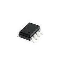
HCPL-2503#320 Avago Technologies US Inc., HCPL-2503#320 Datasheet - Page 12

HCPL-2503#320
Manufacturer Part Number
HCPL-2503#320
Description
OPTOCOUPLER 1MBS UL 8-SMD GW
Manufacturer
Avago Technologies US Inc.
Datasheet
1.HCPL-2503500.pdf
(12 pages)
Specifications of HCPL-2503#320
Input Type
DC
Package / Case
8-SMD Gull Wing
Voltage - Isolation
5000Vrms
Number Of Channels
1, Unidirectional
Current - Output / Channel
8mA
Data Rate
250kbps
Propagation Delay High - Low @ If
1µs @ 8mA
Current - Dc Forward (if)
25mA
Output Type
Open Collector
Mounting Type
Surface Mount, Gull Wing
Isolation Voltage
5000 Vrms
Output Device
Phototransistor
Configuration
1 Channel
Current Transfer Ratio
22 %
Maximum Baud Rate
1 MBps
Maximum Forward Diode Voltage
1.7 V
Maximum Reverse Diode Voltage
5 V
Maximum Input Diode Current
25 mA
Maximum Power Dissipation
100 mW
Maximum Operating Temperature
+ 70 C
Minimum Operating Temperature
0 C
Lead Free Status / RoHS Status
Contains lead / RoHS non-compliant
Available stocks
Company
Part Number
Manufacturer
Quantity
Price
Recommended Circuit Design Parameters
Parameter
Input
Logic Low Output
Voltage – Input Gate
Supply Voltage – Input
Input Resistor
Input Current
Input Current Range
Output
Logic Low Output
Voltage – HCPL-2503
Supply Voltage – Output
Pull-Up Resistor
Required Current Sink
for Logic Low
HCPL-2503 Current
Transfer Ratio
Logic Low Output
Current – HCPL-2503
Data Rate
Notes:
10. The inverting circuit has higher power consumption and must use open collector gates on the input.
11. The load resistor R
12. The maximum current sink required for logic LOW is:
13. The ratio of I
14. The maximum data rate is defined as:
For product information and a complete list of distributors, please go to our website:
Avago, Avago Technologies, and the A logo are trademarks of Avago Technologies Limited in the United States and other countries.
Data subject to change. Copyright © 2007 Avago Technologies Limited. All rights reserved.
AV02-0520EN - June 15, 2007
The selection of R
where I
R
is the current through R
OL
(min) to I
L
L
is the same for both inverting and non-inverting circuits.
must be large enough to guarantee logic LOW and small enough to guarantee logic HIGH under worst case conditions:
OL
(max) gives the design margin for CTR degradation. See Application Note 1002.
Symbol
V
V
R
I
I
V
V
R
I
(max)
CTR
I
(min)
f
L
F
F
OL
OL
D
.
IN
L
OL
CC1
OL
CC2
(A)
(B)
I
OL
V
f
CC
(2503) – I
(max) – V
LSTTL-to-
LSTTL
0.5
5.0
360
430
8
6.75–10
0.5
5.0
20
0.61
11
0.74
250
I
OL
(max) = I
D
IL
= bits/second NRZ
(B)
OL
t
PHL
1
IL
+ t
(B) (max) + I
≤ R
www.avagotech.com
PLH
L
TTL-to-
LSTTL
0.4
5.0
180
200
16
14.0–20 mA
14.5–20
0.5
5.0
8.2
1.0
9
1.26
1.30
250
≤
R
V
I
OH
(max)
CC
(2503) – I
(min) – V
Units
V
V
Ω
mA
V
V
kΩ
mA
%
mA
kb/s
IH
IH
(B)
(B)
Comments
Maximum
± 5%
± 5%
Nominal
Maximum
± 5%
± 5%
Worst Case V
R
Minimum T
+70°C
Worst Case V
T
NRZ, T
A
L
= 0 ° C to +70 ° C
, I
IL
(B)
A
= 25°C
A
= 0˚C to
CC
CC
,
, CTR, I
F
Fig.
8a
8b
8a
8b
8a
8b
Note
11
12
13
14


