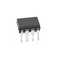
HCPL-3700-500E Avago Technologies US Inc., HCPL-3700-500E Datasheet - Page 10

HCPL-3700-500E
Manufacturer Part Number
HCPL-3700-500E
Description
OTOCOUPLER AC/DC-LOGIC 8-SMD
Manufacturer
Avago Technologies US Inc.
Datasheet
1.HCPL-3700-000E.pdf
(14 pages)
Specifications of HCPL-3700-500E
Voltage - Isolation
3750Vrms
Number Of Channels
1, Unidirectional
Current - Output / Channel
30mA
Propagation Delay High - Low @ If
4µs
Current - Dc Forward (if)
50mA
Input Type
Logic
Output Type
Open Collector
Mounting Type
Surface Mount, Gull Wing
Package / Case
8-SMD Gull Wing
No. Of Channels
1
Optocoupler Output Type
Photodarlington
Input Current
3.7mA
Output Voltage
20V
Opto Case Style
SMD
No. Of Pins
8
Peak Reflow Compatible (260 C)
Yes
Isolation Voltage
3.75kV
Lead Free Status / RoHS Status
Lead free / RoHS Compliant
Available stocks
Company
Part Number
Manufacturer
Quantity
Price
Company:
Part Number:
HCPL-3700-500E
Manufacturer:
AVAGO
Quantity:
10 000
Part Number:
HCPL-3700-500E
Manufacturer:
AVAGO/安华高
Quantity:
20 000
10
Notes:
10. The t
11. The t
12. Common mode transient immunity in Logic High level is the maximum tolerable (positive) dV
13. In applications where dV
14. Logic low output level at Pin 6 occurs under the conditions of V
15. AC voltage is instantaneous voltage.
16. Device considered a two terminal device: Pins 1, 2, 3, 4 connected together, and Pins 5, 6, 7, 8 connected together.
17. In accordance with UL 1577, each optocoupler is proof tested by applying an insulation test voltage ≥ 4500 V rms for 1 second (leakage
18. In accordance with UL 1577, each optocoupler is proof tested by applying an insulation test voltage ≥ 6000 V rms for 1 second (leakage
Figure 1. Typical input characteristics, I
(AC voltage is instantaneous value).
9. All typical values are at T
1. Measured at a point 1.6 mm below seating plane.
2. Current into/out of any single lead.
3. Surge input current duration is 3 ms at 120 Hz pulse repetition rate. Transient input current duration is 10 µs at 120 Hz pulse repetition rate.
4. Derate linearly above 70°C free-air temperature at a rate of 4.1 mW/°C (HCPL-3700/3760) and 3.1 mW/°C (HCPL-0370). Maximum input power
5. Derate linearly above 70°C free-air temperature at a rate of 5.4 mW/°C (HCPL-3700/3760) and 5 mW/°C (HCPL-0370).
6. Derate linearly above 70°C free-air temperature at a rate of 3.9 mW/°C (HCPL-3700/3760) and 1.9 mW/°C (HCPL-0370). Maximum output
7. Derate linearly above 70°C free-air temperature at a rate of 0.6 mA/°C.
8. Maximum operating frequency is defined when output waveform Pin 6 obtains only 90% of V
Note that maximum input power, P
dissipation of 230 mW (HCPL-3700/3760) and 172 mW (HCPL-0370) allows an input IC junction temperature of 125°C at an ambient tempera-
ture of T
power dissipation of 210 mW (HCPL-3700/3760) and 103 mW (HCPL-0370) allows an output IC junction temperature of 125°C at an ambient
temperature of T
wave input signal.
leading edge of the output pulse (see Figure 10).
trailing edge of the output pulse (see Figure 10).
mode pulse, V
level is the maximum tolerable (negative) dV
remain in a Logic Low state (i.e., V
tector IC from destructively high surge currents. The recommended value for R
V
output level at Pin 6 occurs under the conditions of V
detection current limit, I
detection current limit, I
EN/DIN EN 60747-5-5 Insulation Characteristics Table.
CC
) with a minimum value of 240 ý.
PHL
PLH
propagation delay is measured from the 2.5 V level of the leading edge of a 5.0 V input pulse (1 µs rise time) to the 1.5 V level on the
propagation delay is measured from the 2.5 V level of the trailing edge of a 5.0 V input pulse (1 µs fall time) to the 1.5 V level on the
A
= 70°C. Excessive P
CM
, to insure that the output will remain in a Logic High state (i.e., V
A
= 70°C.
A
i-o
i-o
CM
= 25°C, V
≤ 5 µA).
≤ 5 µA). This test is performed before the 100% production test for partial discharge (Method b) shown in the IEC/
/dt may exceed 50,000 V/µs (such as static discharge), a series resistor, R
IN
and T
IN
O
vs. V
CC
< 0.8 V). See Figure 11.
IN
J
, must be observed.
may result in IC chip degradation.
= 5.0 V unless otherwise stated.
IN
CM
Figure 2. Typical transfer characteristics.
Input Signal
I
V
V
/dt on the trailing edge of the common mode pulse signal, V
TH
TH(DC)
TH(AC)
IN
V
TH-
as well as the range of V
IN
Device
HCPL-0370/3700
HCPL-3760
ALL
ALL
ž V
TH+
as well as the range of V
CC
O
is 240 ý per volt of allowable drop in V
> 2.0 V). Common mode transient immunity in Logic Low
IN
< V
TH+
2.5 mA
1.2 mA
3.7 V
4.9 V
TH+
once V
CC
CM
IN
/dt on the leading edge of the common
with R
> V
CC
IN
, should be included to protect the de-
TH–
has decreased below V
L
once V
= 4.7 kW, C
TH–
1.3 mA
0.6 mA
2.6 V
3.7 V
CM
, to insure that the output will
IN
has exceeded V
L
= 30 pF using a 5 V square
CC
Input Connection
PINS 2, 3 OR 1, 4
PINS 2, 3
PINS 1, 4
(between Pin 8 and
TH-
.
TH+
. Logic high


