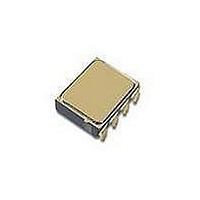
HCPL-5121-100 Avago Technologies US Inc., HCPL-5121-100 Datasheet - Page 4

HCPL-5121-100
Manufacturer Part Number
HCPL-5121-100
Description
ISOLAT 1.5KVDC 1CH TOTEM 8SMD BJ
Manufacturer
Avago Technologies US Inc.
Datasheet
1.HCPL-5120.pdf
(16 pages)
Specifications of HCPL-5121-100
Output Type
Push-Pull, Totem-Pole
Package / Case
8-SMD Butt Joint
Voltage - Isolation
1500VDC
Number Of Channels
1, Unidirectional
Current - Output / Channel
2A
Propagation Delay High - Low @ If
300ns @ 10mA ~ 18mA
Current - Dc Forward (if)
25mA
Input Type
DC
Mounting Type
Surface Mount
Configuration
1 Channel
Maximum Propagation Delay Time
500 ns
Maximum Forward Diode Voltage
1.8 V
Minimum Forward Diode Voltage
1.2 V
Maximum Reverse Diode Voltage
5 V
Maximum Forward Diode Current
18 mA
Maximum Power Dissipation
295 mW
Maximum Operating Temperature
+ 125 C
Minimum Operating Temperature
- 55 C
Number Of Elements
1
Forward Voltage
1.8V
Forward Current
25mA
Package Type
PDIP
Operating Temp Range
-55C to 125C
Power Dissipation
295mW
Propagation Delay Time
500ns
Pin Count
8
Mounting
Surface Mount
Reverse Breakdown Voltage
5V
Operating Temperature Classification
Military
Lead Free Status / RoHS Status
Contains lead / RoHS non-compliant
Lead Free Status / RoHS Status
Lead free / RoHS Compliant, Contains lead / RoHS non-compliant
Absolute Maximum Ratings
Notes:
. No derating required for typical case-to-ambient thermal resistance
2. Maximum pulse width = 0µs, maximum duty cycle = 0.2%. This value is intended to allow for component tolerances for designs with I
3. Derate linearly above 02°C free air temperature at a rate of 6mW/°C for typical case-to-ambient thermal resistance
4. Derate linearly above 02°C free air temperature at a rate of 6mW/°C for typical case-to-ambient thermal resistance
ESD Classification
Recommended Operating Conditions
4
Parameter
Storage Temperature
Operating Temperature
Case Temperature
Junction Temperature
Lead Solder Temperature
Average Input Current
Peak Transient Input Current
(<1 µs pulse width, 300 pps)
Reverse Input Voltage
“High” Peak Output Current
“Low” Peak Output Current
Supply Voltage
Output Voltage
Emitter Power Dissipation
Output Power Dissipation
Total Power Dissipation
MIL-STD-883, Method 305
Parameter
Power Supply Voltage
Input Current (ON)
Input Voltage (OFF)
Operating Temperature
Figure 36.
Figure 35 and 36.
minimum = 2.0A. See Applications section for additional details on limiting I
(V
Symbol
( ), Class
V
CC
I
F (ON)
F (OFF)
T
– V
A
EE
Symbol
(V
I
I
V
)
OH (PEAK)
OL (PEAK)
I
O (PEAK)
CC
I
F AVG
V
P
T
T
T
F PK
P
P
T
-V
S
A
C
O
J
R
E
T
EE
)
(θ
CA
Min.
-65
-55
Min.
=40°C/W). Refer to Figure 35.
-3.0
-55
0
0
15
10
OH
peak.
260 for 10s
+150
+125
+145
+150
Max.
VCC
250
295
1.0
2.5
2.5
25
35
45
5
Max.
125
0.8
30
18
Units
mW
mW
mW
mA
°C
°C
°C
°C
°C
A
V
A
A
V
V
(θ
(θ
CA
CA
=40°C/W). Refer to
=40°C/W). Refer to
Units
Volts
Volts
mA
°C
Note
1
2
2
1
3
4
O
peak


