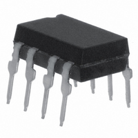
IL300-DEFG Vishay, IL300-DEFG Datasheet - Page 8

IL300-DEFG
Manufacturer Part Number
IL300-DEFG
Description
OPTOCOUPLER HI GAIN WIDE BW 8DIP
Manufacturer
Vishay
Specifications of IL300-DEFG
Mounting Type
Through Hole
Isolation Voltage
5300 Vrms
Number Of Channels
2
Input Type
DC
Voltage - Isolation
5300Vrms
Current Transfer Ratio (min)
0.77% @ 10mA
Current Transfer Ratio (max)
1.18% @ 10mA
Current - Dc Forward (if)
60mA
Output Type
Linear Photovoltaic
Package / Case
8-DIP (0.300", 7.62mm)
Current Transfer Ratio
0.5 % to 1.1 %
Forward Current
10 mA
Maximum Fall Time
1.75 us
Maximum Rise Time
1.75 us
Output Device
PIN Photodiode
Configuration
1 Channel
Maximum Forward Diode Voltage
1.5 V
Maximum Reverse Diode Voltage
5 V
Maximum Input Diode Current
60 mA
Maximum Power Dissipation
210 mW
Maximum Operating Temperature
+ 100 C
Minimum Operating Temperature
- 55 C
No. Of Channels
1
Optocoupler Output Type
Photodiode
Input Current
10mA
Output Voltage
50V
Opto Case Style
DIP
No. Of Pins
8
Gain Db Max
1.181dB
Lead Free Status / RoHS Status
Lead free / RoHS Compliant
Voltage - Output
-
Current - Output / Channel
-
Vce Saturation (max)
-
Lead Free Status / Rohs Status
Lead free / RoHS Compliant
Other names
751-1293-5
IL300-DEFGGI
IL300-DEFGGI
IL300-DEFGGI
IL300-DEFGGI
Available stocks
Company
Part Number
Manufacturer
Quantity
Price
Company:
Part Number:
IL300-DEFG
Manufacturer:
Vishay
Quantity:
2 000
IL300
Vishay Semiconductors
Table 1. Gives the value of R5 given the production K3 bin.
The last step in the design is selecting the LED current
limiting resistor (R4). The output of the operational amplifier
is targeted to be 50 % of the V
quiescent current of 12 mA the typical LED (V
Given this and the operational output voltage, R4 can be
calculated.
The circuit was constructed with an LM201 differential
operational amplifier using the resistors selected. The
amplifier was compensated with a 100 pF capacitor
connected between pins 1 and 8.
The DC transfer characteristics are shown in figure 17. The
amplifier was designed to have a gain of 0.6 and was
measured to be 0.6036. Greater accuracy can be achieved
by adding a balancing circuit, and potentiometer in the input
divider, or at R5. The circuit shows exceptionally good gain
linearity with an RMS error of only 0.0133 % over the input
voltage range of 4 V to 6 V in a servo mode; see figure 15.
www.vishay.com
8
R4 =
TABLE 1 - R5 SELECTION
V
opamp
BIN
I
A
B
C
D
G
H
E
F
J
Fq
I
- V F
=
2.5 V - 1.3 V
12 mA
CC
For technical questions, contact:
, or 2.5 V. With an LED
0.560
0.623
0.693
0.769
0.855
0.950
1.056
1.175
1.304
1.449
MIN.
= 100 Ω
Linear Optocoupler, High Gain
Stability, Wide Bandwidth
F
) is 1.3 V.
17096
0.623
0.693
0.769
0.855
0.950
1.056
1.175
1.304
1.449
1.610
MAX.
K3
optocoupleranswers@vishay.com
The AC characteristics are also quite impressive offering a
- 3 dB bandwidth of 100 kHz, with a - 45° phase shift at
80 kHz as shown in figure 16.
iil300_19
iil300_20
- 0.005
- 0.010
- 0.015
0.025
0.020
0.015
0.010
0.005
0.000
3.75
3.50
3.25
3.00
2.75
2.50
2.25
Fig. 15 - Linearity Error vs. Input Voltage
4.0
4.0
V
LM201
out
0.59
0.66
0.73
0.81
0.93
1.11
1.24
1.37
1.53
TYP.
Fig. 14 - Transfer Gain
= 14.4 mV + 0.6036 x V
LM 201 T
1
V
4.5
4.5
in
- Input Voltage (V)
a
= 25 °C
5.0
5.0
Document Number: 83622
in
5.5
5.5
R5 RESISTOR
Rev. 1.6, 10-Nov-10
1 %
51.1
45.3
41.2
37.4
32.4
19.4
30
27
24
22
6.0
6.0
kΩ


