TCET4100 Vishay, TCET4100 Datasheet
TCET4100
Specifications of TCET4100
TCET4100


Related parts for TCET4100

TCET4100 Summary of contents
Page 1
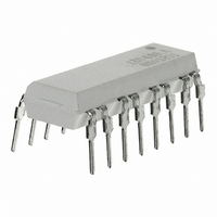
... PIN 17198 Description The TCET2100/ TCET4100 consists of a phototrans- istor optically coupled to a gallium arsenide infrared- emitting diode, available in 8 pin (dual channel) and 16 pin (quad channel) package. The elements are mounted on one leadframe provid- ing a fixed distance between input and output for high- est safety requirements ...
Page 2
... TCET2100 / TCET4100 Vishay Semiconductors Absolute Maximum Ratings °C, unless otherwise specified amb Stresses in excess of the absolute Maximum Ratings can cause permanent damage to the device. Functional operation of the device is not implied at these or any other conditions in excess of those given in the operational sections of this document. Exposure to absolute Maximum Rating for extended periods of the time can adversely affect reliability ...
Page 3
... Routine test Partial discharge test voltage - Lot test (sample test) (see figure 2) Insulation resistance V = 500 500 500 (construction test only) Document Number 83727 Rev. 1.4, 26-Oct-04 TCET2100 / TCET4100 Test condition Symbol = CEsat = 10 mA Test condition Symbol = 5 mA CTR F Test condition Symbol ...
Page 4
... TCET2100 / TCET4100 Vishay Semiconductors 300 Phototransistor 250 Psi ( mW ) 200 150 100 IR-Diode 50 Isi ( 100 125 – Safety Temperature ( ° 9182 si Figure 1. Derating diagram Switching Characteristics Parameter Delay time (see figure 3) Rise time (see figure 3) Turn-on time (see figure 3) Storage time (see figure 3) ...
Page 5
... V - Forward Voltage ( 11862 F Figure 7. Forward Current vs. Forward Voltage Document Number 83727 Rev. 1.4, 26-Oct-04 TCET2100 / TCET4100 96 11698 t t storage time fall time turn-off time 2.0 1.5 1.0 0.5 0 –25 ...
Page 6
... TCET2100 / TCET4100 Vishay Semiconductors 100 V = 0.1 0.01 0 – Forward Current ( 11027 F Figure 10. Collector Current vs. Forward Current 100 20mA I =50mA F 10mA 10 5mA 2mA 1 1mA 0.1 0 – Collector Emitter Voltage ( 10985 CE Figure 11. Collector Current vs. Collector Emitter Voltage 2.4 High Efficiency Red 2.0 1.6 1 ...
Page 7
... Package Dimensions in mm Package Dimensions in mm Document Number 83727 Rev. 1.4, 26-Oct-04 TCET2100 / TCET4100 Vishay Semiconductors 14784 14783 www.vishay.com 7 ...
Page 8
... TCET2100 / TCET4100 Vishay Semiconductors Ozone Depleting Substances Policy Statement It is the policy of Vishay Semiconductor GmbH to 1. Meet all present and future national and international statutory requirements. 2. Regularly and continuously improve the performance of our products, processes, distribution and operatingsystems with respect to their impact on the health and safety of our employees and the public, as well as their impact on the environment ...
Page 9
... Vishay disclaims any and all liability arising out of the use or application of any product described herein or of any information provided herein to the maximum extent permitted by law. The product specifications do not expand or otherwise modify Vishay’ ...